
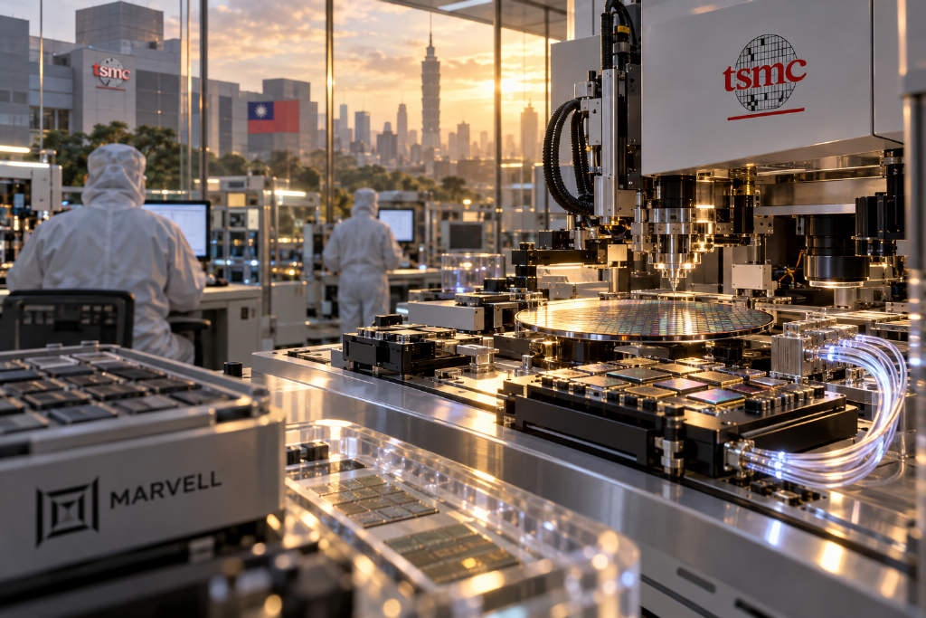
Silicon Photonics Bottleneck Shifts: From Materials to Packaging Precision
At the Semicon Network Summit 2026, industry representatives said the choke point in silicon photonics is no longer materials. It has moved to packaging precision and heterogeneous integration, DIGITIMES reported. So yes, the story is changing: less about material R&D, more about hard manufacturing process problems.
Marvell: Copper Interconnects Nearing Physical Limits, Optical Interconnects Inevitable
Marvell's CTO said copper interconnects are getting close to their physical limits, which makes end-to-end optical interconnects unavoidable. The company is speeding up its silicon photonics chip work. And it said its dependence on the Taiwan supply chain is increasing.
CPO Challenge: Integrating Optical Materials with CMOS Platforms
TNO/Holst Centre said the real problem in co-packaged optics (CPO) is integrating optical materials like LiNbO₃ and InP with CMOS platforms. That means packaging processes need breakthroughs in heterogeneous integration capability. Hard stuff.
Taiwan's Packaging Advantage: Micron-Level Fiber Alignment Precision
TSIA said packaging processes now demand micron-level fiber alignment precision, and Taiwan is ahead globally in chip and packaging technologies. TNO added that panel-level packaging is a major opening for Taiwan, using its experience with large glass substrates to help meet the huge demand for data center optical interconnects. But the equipment shortfall is still there, especially in Chip-to-Wafer bonding tools.