
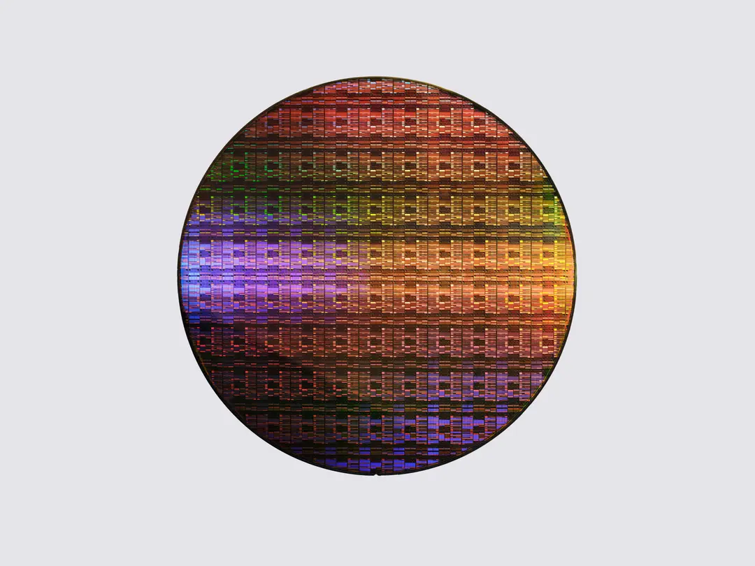
IBM has introduced what it calls the world’s first 0.7nm chip technology, built on a new Nanostack three-dimensional nanosheet architecture. The company said a single chip can integrate nearly 100 billion transistors, reaching twice the density of its 2nm generation, with mass production possible in as little as five years.
The announcement was made at the VLSI 2026 research conference. IBM’s pitch is clear: instead of continuing to shrink transistors along the traditional planar path, the company is stacking multiple transistor layers vertically and optimizing each layer independently for materials and performance.
IBM shifts from shrinking transistors to stacking them
Nanostack is described as a three-dimensional, nanosheet-based design. Nanosheet transistors were already part of the leading edge in chip architecture, and IBM’s latest step adds a vertical layer to that foundation. IBM research director Jay Gambetta said the work is not just about making smaller transistors, but about reinventing how chips are built.
IBM said it validated the approach through three technical demonstrations: CMOS integration using ultrathin dielectric bonding, a dual-channel engineering demonstration, and the operation of a CMOS inverter. That last result matters because the inverter is one of the most basic building blocks in digital logic, showing the design can function in a real circuit environment.
SRAM shrinks by 40% as AI workloads drive demand
A VLSI paper presented alongside the announcement said the Nanostack design reduces SRAM area by 40%. For AI inference, SRAM density is a major factor because model weights must be accessed repeatedly and at high speed. A smaller SRAM footprint means more cache can fit into the same chip area, or similar cache capacity can be maintained with lower power use.
IBM also compared the technology with its 2nm chip generation. At the same power level, performance can improve by up to 50%. At the same performance level, power consumption can drop by up to 70%. Those figures point directly to the power and cooling costs tied to large-scale AI training clusters.
0.7nm is a process generation label, not a literal width
When IBM announced its 2nm technology in 2021, it described the milestone as fitting 50 billion transistors into a fingernail-sized chip. The new 0.7nm generation pushes that figure to nearly 100 billion in the same area. IBM also noted that “0.7nm” should not be read as the exact physical width of a transistor. In current semiconductor terminology, the node name functions as a generation label tied to gains in density, performance, and energy efficiency.
IBM’s production timeline remains flexible. The company said the technology could enter mass production in as little as five years, though actual deployment will still depend on yield, supply chain conditions, and customer demand. IBM also said it plans to build the world’s first pure quantum computer wafer foundry, called Anderon, showing that its research efforts are moving across multiple technology tracks at once.