
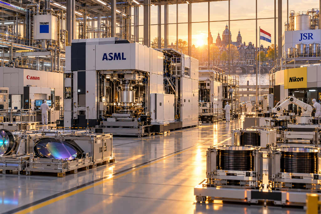
Lithography suppliers are entering another round of expansion, product development, and price adjustments as chipmakers keep placing orders across multiple parts of the semiconductor stack. On Oct. 21, Canon said output of its semiconductor lithography tools next year could rise to nearly double this year’s level. A day earlier, Nikon said it had started development of a higher-precision digital lithography system aimed at the advanced packaging market.
ASML had already signaled the scale of demand in its third-quarter earnings release a week earlier. The company said customer demand for 2027 and 2028 tools has moved beyond its current capacity expansion plan, and customers have even started asking about supply in 2029 and 2030. ASML plans to increase capacity for low-NA EUV and immersion DUV by 30% each next year, while exploring whether growth can top 30% in the following year. It also said pricing negotiations with major customers have been completed and some key products will become more expensive.
Upstream suppliers are moving in the same direction. Trumpf expects both orders and revenue in its EUV business to post double-digit growth in the new fiscal year. JSR, for its part, completed a South Korean plant at the end of September for the final production step of metal oxide resist, or MOR.
Capacity growth is spreading beyond EUV
Canon said it will use facilities including its new Utsunomiya plant, completed last year, to carry out the production increase. Hiroaki Takeishi, who oversees the industrial equipment business, said in an Oct. 21 interview that chipmakers are continuing to invest not only in Taiwan, South Korea, and mainland China, but in multiple regions globally, and that demand could continue through 2028. Canon’s i-line lithography tools are used in parts of the manufacturing flow for memory and power devices, and expansion in those markets is lifting equipment demand as well.
In advanced back-end lithography, Canon said inquiries for its tools have surged since the middle of 2025. The company recently disclosed a plan to raise capacity for those systems by 50% by 2029 compared with 2026, while continuing development of products for larger substrates. As package sizes increase, interconnect lines between chips have to be formed over a wider area. That means tool vendors need not only more output, but also systems that can handle larger substrates.
On the wafer manufacturing side, Micron on Oct. 21 laid out its next DRAM process steps. Its 1γ node, which uses EUV, has entered mass production, and the next-generation 1δ node is scheduled for volume ramp in the second half of 2027. ASML expects equipment sales to memory customers to grow about 75% this year, versus roughly 10% for logic customers. In explaining the memory increase, the company pointed to two drivers directly: customer capacity additions and greater use of EUV in advanced DRAM processes.
ASML expects to produce about 65 low-NA EUV systems this year. For immersion DUV, where it had originally planned a reduction, the company has now revised its delivery target to a level roughly in line with last year. To keep expanding supply, ASML still needs to rework existing factory space and shorten assembly and testing time. The first phase of its new campus in Eindhoven is expected to come online in 2029, so near-term output growth will still rely mainly on current facilities.
On orders, ASML said it has already started receiving bookings for 2028. It has not yet accepted formal orders tied to purchase intentions for 2029 and 2030. The company said it first needs to consolidate demand across customers and compare that with the capacity it expects to have available, so it does not commit supply too early to some buyers at the expense of long-term customers.
ASML’s installed base business, including services and field options, generated about 3.3 billion euros in third-quarter revenue, around 400 million euros above guidance. Most of that upside came from upgrades. Customers can raise throughput on installed tools through upgrades and gain additional wafer capacity without first adding the same amount of fab space.
At the start of 2027, ASML also plans a limited launch of the NXE:3800F, which will raise wafer throughput from 230 wafers per hour on the previous generation to 260 wafers per hour. Its next-generation immersion DUV tool for critical layers will lift that figure to 330 wafers per hour. For customers, buying more machines and getting more wafers out of each machine are now moving forward at the same time.
Those new systems and upgrade products are also part of ASML’s latest pricing round. The company said talks with major customers are complete. The price increases mainly target high-end volume production products, and upgrade products will also see price adjustments. The effect will show up partly in 2027 and fully in 2028. ASML did not disclose a uniform increase rate. Customers still have to weigh delivery timing, upgrade spending, and incremental wafer output, with tool price being only one factor.
Nikon and Canon are looking for growth in new segments
On Oct. 13, Nikon unveiled the DSP-110 digital lithography system, with commercial release planned for April 2027. The company had already begun taking orders for the DSP-100 in July last year, combining semiconductor exposure technology with multi-lens technology used in flat-panel displays to enter the back-end lithography market.
These systems target large interposers and multilayer package substrates. Once multiple chips are placed in the same package, denser interconnects are needed between them and package size expands. Exposure tools then have to balance wiring precision with large-area processing. Nikon is applying its existing strengths in precision exposure and large-area exposure to this market, aiming at packaging investment rather than competing head-on with EUV in front-end nanometer transistor fabrication.
The DSP-110 uses maskless digital lithography, so customers do not need to make a physical photomask for every circuit pattern. It can process large square substrates and also supports 300 mm wafers. When packaging houses revise wiring designs, they can cut out part of the preparation work tied to making new masks. Support for different substrate formats also gives customers more room to adjust production plans later.
The new tool has a line-and-space resolution of 1.5 μm and can process 72 substrates per hour on a 510 mm × 515 mm substrate, about 40% faster than the previous generation. The earlier model had 1.0 μm resolution. Nikon redesigned the optical system this time, prioritizing production speed and widening the allowable focus offset range so the tool can better handle different substrate surface conditions.
If current wiring requirements are already sufficient, higher hourly output can help lower processing cost. If finer lines are needed later, the DSP-110 can be upgraded to 1.0 μm by replacing the optical system.
On Oct. 20, Nikon said it had started development of a 0.5 μm digital lithography system and had secured support from Japan’s New Energy and Industrial Technology Development Organization. The project targets large-area, high-precision exposure for advanced packaging and aims to control layer-to-layer alignment error within ±0.15 μm, half the level of existing products. Nikon has not provided a commercialization timetable.
Canon, beyond expanding supply of its current lithography tools, is also pushing nanoimprint technology for wafer manufacturing. On Oct. 1, the company said that customers using its nanoimprint equipment, introduced in 2023, are making final adjustments to optimize mass-production lines. Engineers described the specific issues that still need to be solved after the tools are installed at customer sites.
Nanoimprint transfers the required pattern by pressing a template carrying circuit features directly onto resin on the wafer surface. It removes the need for complex projection exposure, but the contact process introduces problems such as particle contamination and template damage. Chips are built from multiple stacked layers, and those layers also have to align accurately. Printing fine lines in a single step is not enough by itself to complete mass production.
Canon engineers said contact can become unstable when a square template is used at the edge of a round wafer. The team has to adjust not only the imprint process itself, but also account for the effect of later steps such as etching on the pattern. One engineer responsible for system control said the team analyzed more than a month of data to identify the source of subtle errors and then addressed them through hardware changes in order to reach the pattern transfer precision required for mass production.
Canon also needs to work with group companies to improve supporting equipment such as template cleaning systems, extend template life, and fold maintenance costs into customer cost calculations. The nanoimprint effort has moved beyond showing single-tool performance and into full-line coordination. The company has not disclosed the scale of mass production, yield, or formal production start dates for those customers, and future equipment purchases will depend on actual operating results after adoption.
Light sources and materials suppliers are also expanding
On Oct. 15, Germany’s Trumpf reported fiscal-year results through the end of June. Revenue from its EUV business reached 791 million euros, up 9.2% year over year, compared with 0.2% growth for the company overall. Trumpf supplies ASML with high-power drive lasers. Those lasers hit tin droplets to create plasma, which then generates the extreme ultraviolet light needed for exposure.
In its latest annual report, Trumpf described its next-generation MK5 high-power laser. The company highlighted not only performance, but also faster installation and more stable operation. With modular design, more sensors, and diagnostic systems, service teams can identify faults more quickly and reduce downtime. For a fab trying to increase wafer output, the ability of the light source to keep running matters as much as the scanner’s rated throughput.
Trumpf expects both orders and revenue in its EUV business to post double-digit growth in fiscal 2026/27. As customers raise wafer output, light-source suppliers have to keep pace in both equipment delivery and field maintenance.
JSR’s latest move is centered on materials supply. Its Ochang plant in South Korea, completed on Sept. 30, will handle the final production step for metal oxide resist, or MOR. The company said the goal is to strengthen local manufacturing and quality assurance and respond more quickly to the needs of major South Korean customers.
When the project was announced in 2024, JSR had already cited the possibility that major South Korean customers would adopt MOR and had planned to start operations in 2026. With construction now complete, one of the local supply conditions needed for customer adoption has moved forward. Early investment in production allows materials suppliers to prepare shipments alongside new process development at fabs, though the actual nodes and volumes customers will use have not been disclosed.
Photoresist preserves the pattern formed during exposure, and material response affects whether line edges remain smooth and whether adjacent lines accidentally bridge. In its annual report released the same day, JSR said different customers’ process and equipment conditions require tailored support from materials suppliers. Locating production, quality assurance, and technical support close to customers is not only about shorter transport distance, but also about solving on-site issues faster.
JSR plans to expand revenue from its electronic materials business to 1.7 times its fiscal 2025 level by fiscal 2030, with lithography materials remaining a main growth driver. The South Korean plant is one step in strengthening production in Asia and coordination with customers. As chipmakers settle on new processes and prepare for volume ramps, materials suppliers need to enter development and validation early if they want to secure long-term supply business later.
Longer-term research is still moving ahead
For more distant process evolution, ASML and Zeiss researchers proposed a Hyper NA system concept in a paper published in October, with a numerical aperture of at least 0.75, above the 0.55 used in current high-NA EUV systems. One of the research goals is to reuse as much of the existing light source, mask, and equipment manufacturing infrastructure as possible.
Neither company has committed to putting that concept into production. At this stage, it remains part of preparatory work for a next-generation system.
Across front-end exposure, packaging interconnect patterning, and materials support, the lithography supply chain is taking in a new wave of customer spending. Upgrades to installed tools are already contributing to current revenue, while new capacity, product launches, and process introductions are progressing on different timelines. Whether suppliers can turn this investment cycle into sustained revenue will still depend on delivery, mass-production validation, and stable supply.