
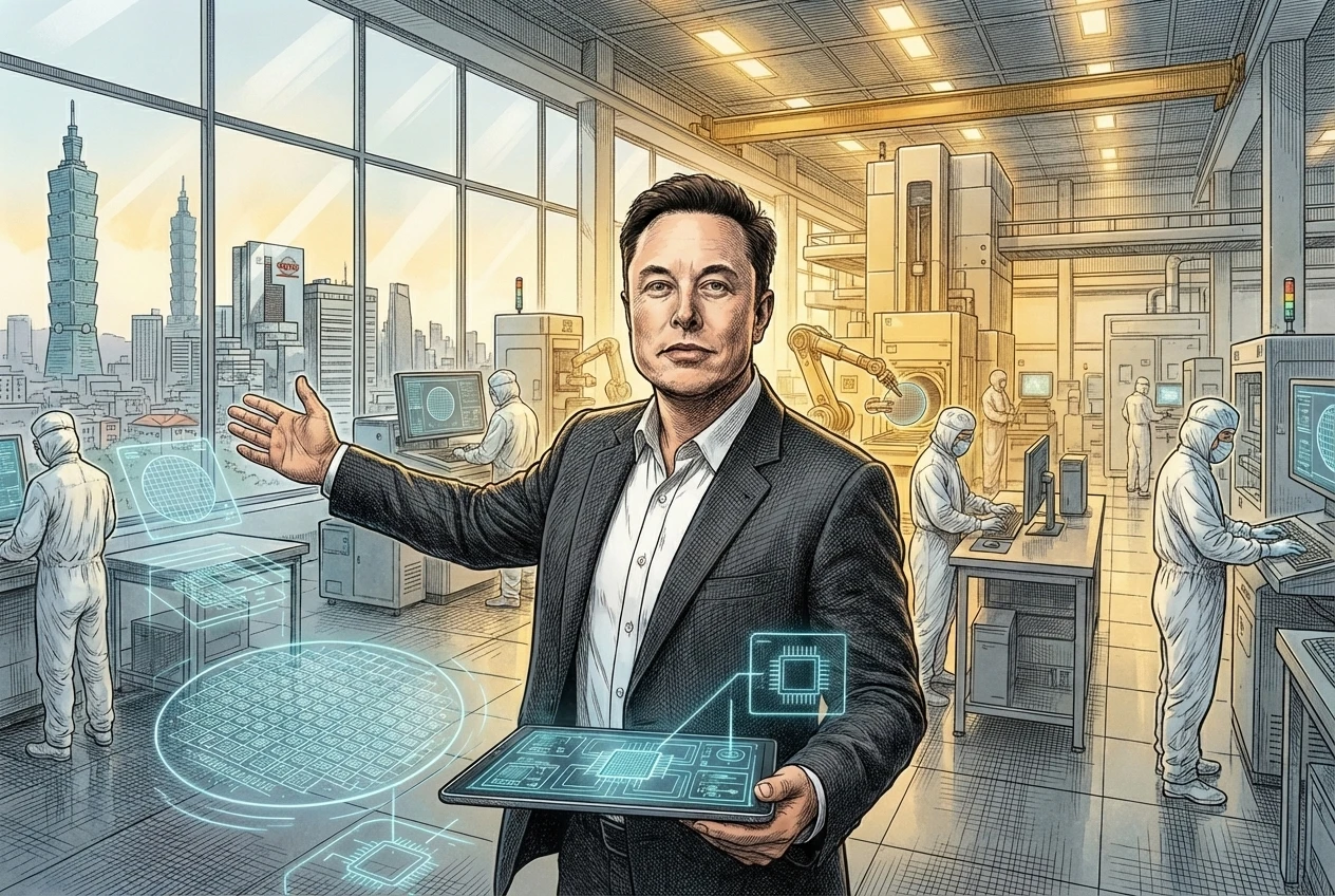
Elon Musk said on X that the TeraFab project will launch in 7 days. Based on the details cited so far, the plan is to build a massive semiconductor manufacturing facility in the United States with a targeted annual output of 100 billion to 200 billion chips, a scale claimed to exceed the combined capacity of TSMC’s Taiwan fabs.
That headline number immediately shifts attention to a basic question: is Musk about to unveil an executable manufacturing program with a defined roadmap, or is this another concept-first announcement waiting for operational details. At this stage, the ambition is clear. So is the gap between a bold target and a working fab.
Tesla’s chip demand sits at the center of the plan
The source material frames TeraFab as a response to Tesla’s long-running chip constraints. Pressure has built across several fronts, from the production struggles tied to Model 3 to Dojo supercomputer expansion and the expected scale-up of the Optimus robot program. All of them require advanced chips, and existing supply chains have not kept pace with that demand.
Foundry schedules at TSMC and Samsung remain tight, while NVIDIA and AMD are also competing for capacity. For Tesla, dependence on outside fabrication leaves major business lines exposed to the same bottleneck. If TeraFab moves beyond the announcement stage, the strategic purpose is plain: gain tighter control over a critical part of the stack.
Cleanroom comments triggered industry backlash
Debate started even before a formal launch. Musk had previously suggested the idea of a 2nm fab that would not need traditional cleanroom infrastructure, and he even said he could “smoke a cigar in the fab.” Those remarks drew a sharp reaction from semiconductor professionals.
The reason is straightforward. At 2nm, tolerance for particle contamination is extremely low, and dust, skin flakes, or ash can ruin wafers at scale. The source notes that industry participants see cleanrooms not as conservative habit but as an engineering necessity. That is why scrutiny around TeraFab is focused not only on the size of the proposal, but on whether the manufacturing concept respects the physical limits of chip production.
Why the 200 billion target is facing pushback
The production goal itself is one of the biggest sticking points. The source says TSMC shipped roughly 30 billion to 40 billion chips in 2024, while TeraFab is described as a new facility aiming for 100 billion to 200 billion chips annually. Set side by side, those figures raise obvious questions about construction time, capital intensity, and access to process technology.
Without a major process breakthrough, reaching that level of output would imply enormous investment and a buildout measured in years. That is the core of the skepticism. The target is dramatic, but the path to making it real looks expensive, slow, and technically demanding.
Three routes analysts see as more realistic
From an execution standpoint, the source outlines three possible paths being discussed. One is to secure technology licensing from existing chipmakers such as Intel or TSMC rather than developing the entire process stack from scratch. Another is to deepen cooperation with Intel Foundry Services and rely on Intel’s current fabs and process capabilities to accelerate expansion. A third option is capital injection into existing production lines in exchange for priority access to capacity.
All three approaches point in the same direction. They rely on integration, partnership, or financial leverage rather than any break from core fab requirements. If TeraFab is meant to move quickly, it would likely have to build on the current semiconductor system instead of trying to replace it overnight.
U.S. localization policy forms the broader backdrop
The timing also matters. The source ties TeraFab to the broader push for domestic semiconductor manufacturing in the United States. If Musk presents the project as a way to reduce strategic reliance on Taiwan-based chip production, that framing could align with current policy incentives. Rising AI compute demand adds another layer of justification for new capacity.
Tesla, NVIDIA, and AMD are all waiting in front of the same supply constraint. Even partial substitute capacity would create room in the market. What the industry is waiting for now is not another slogan, but the substance of what Musk plans to show in seven days.