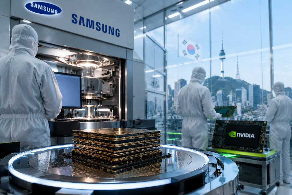
Samsung Electronics is developing an 8-layer HBM4E, or seventh-generation high-bandwidth memory, product tailored to Nvidia’s requirements, according to a report by Seoul Economic cited by ChainCatcher. The effort is aimed at securing a core partner position in the supply chain for Nvidia’s custom NVHBM memory. The report says the new design lowers stack height compared with Samsung’s earlier 12-layer and 16-layer plans, while targeting speeds of 17-18Gbps, about 20% above the 14.4Gbps level of Samsung’s initial HBM4E samples. Nvidia is said to be planning the memory for NVHBM built around its publicly disclosed NVLink-optimized specifications. Seoul Economic also said the 8-layer approach runs against the usual HBM strategy of increasing capacity through more stacked layers, but could ease backend process complexity and reduce yield pressure, making it easier to expand supply. The report added that Nvidia may use that design choice to address memory shortages. NVHBM could begin shipping with Rubin Ultra, Nvidia’s next-generation AI GPU expected next year, which would expand GPU-to-GPU interconnect scale from 72 to as many as 576. In the custom HBM market, the report said Samsung may hold an edge over SK hynix and Micron because NVHBM requires both DRAM capability and logic-die-based base die design and manufacturing.
Samsung Electronics is developing an 8-layer HBM4E, the seventh generation of high-bandwidth memory, to meet Nvidia’s requirements and win a core partner role in supplying its custom NVHBM memory, according to Seoul Economic in a report cited by ChainCatcher.
The report said the product lowers stack height from Samsung’s original 12-layer and 16-layer plans. Nvidia’s target specification is 17-18Gbps, roughly 20% faster than the 14.4Gbps speed of Samsung’s early HBM4E samples. The memory is expected to be used for NVHBM based on Nvidia’s publicly disclosed NVLink-optimized specifications.
An 8-layer design instead of taller stacks
That approach runs against the usual HBM playbook, where suppliers raise capacity by increasing the number of stacked layers. Seoul Economic said the 8-layer design could reduce backend process difficulty and ease yield pressure. That, in turn, would help expand supply and is seen as part of Nvidia’s strategy to relieve memory shortages.
Rubin Ultra seen as the first deployment point
The report said NVHBM could be adopted starting with Rubin Ultra, Nvidia’s next-generation AI GPU expected next year. Rubin Ultra is described as expanding GPU-to-GPU interconnect scale from 72 to as many as 576, using hundreds of GPUs equipped with faster HBM to lift overall computing performance.
Samsung’s position in custom HBM
In the custom HBM segment, the report said Samsung is viewed as more competitive than SK hynix and Micron because NVHBM requires both DRAM capability and the ability to design and manufacture a logic-chip-based base die in an integrated manner.
Industry sources cited in the report also said Samsung has already validated industry-leading speed levels in HBM4, which could give it an edge in the race on performance.
This article was originally published by Bit.Fan. For more cryptocurrency news and market insights, visit www.bit.fan. Disclaimer:
The market information, project data, and third-party content displayed on this platform are for industry information sharing only and do not constitute any form of investment advice or return commitment.
Cryptocurrency trading carries high risks. Users should fully assess their risk tolerance and make independent decisions. All profits, losses, and legal responsibilities are borne by the users themselves.