
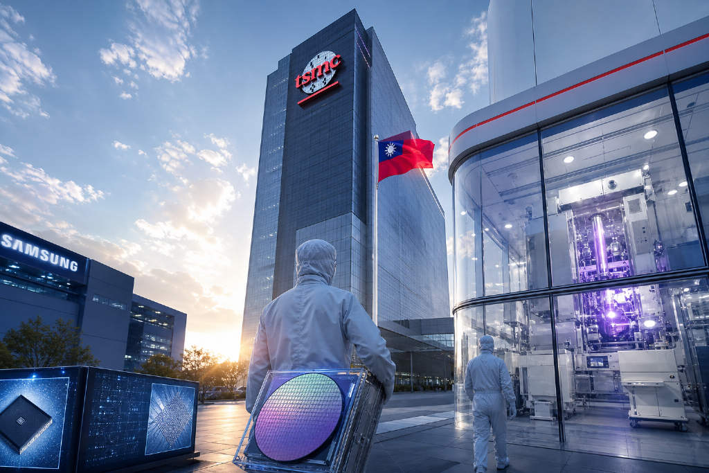
Samsung Foundry has revised its leading-edge roadmap, pushing mass production of its 1.4nm process to 2029 from an earlier 2027 target. Before it gets there, the company will keep expanding and refining its 2nm platform, with the next few years centered on process maturity, yield improvement and customer adoption.
Samsung had outlined the 2027 target for 1.4nm back in 2022. Moving that goal to 2029 puts the schedule 2 years behind the original plan and leaves Samsung with another 3 years to deepen work on its 2nm platform.
Samsung shifts from aggressive node timing to extending 2nm
Samsung had long taken a relatively aggressive approach in advanced process technology. At the 3nm node, it moved early to gate-all-around, or GAA, transistors in an effort to build differentiation and close the gap with Taiwan Semiconductor Manufacturing Co. (TSMC) through faster node transitions.
That equation looks different in the 2nm era. The technical difficulty and capital required for advanced manufacturing are rising quickly, and the contest is no longer just about who reaches the next node first.
For a foundry, the value of a new node depends on whether it can deliver yield, performance, power efficiency, customer volume and production cost at scale. In that context, the article argues that it makes more sense for Samsung to mature its 2nm platform first and extend its commercial life through derivative processes instead of forcing an early move to 1.4nm.
That does not mean Samsung is standing still at 2nm. Beyond its baseline SF2 process, the company is developing derivative 2nm technologies for different applications and plans to introduce backside power delivery in more advanced versions. For AI and high-performance computing, or HPC, chips, growing die sizes and power demands are making power delivery a bigger performance factor. By that logic, Samsung’s main task over the next few years is not simply to tape out 1.4nm as fast as possible, but to turn 2nm into a mature, reliable platform capable of high-volume shipments.
Why Samsung is not rushing High-NA EUV
Samsung is also not treating High-NA EUV, or high numerical aperture extreme ultraviolet lithography, as a mandatory production technology for 2nm and 1.4nm. Samsung Electronics Vice President Park Chang-min previously said the company wants to apply High-NA EUV to mass production at advanced nodes such as 2nm and 1.4nm in the future, but the technology still needs to mature.
Samsung’s view is that High-NA EUV may only become truly necessary for advanced-node production starting at A10 and below, meaning the 1nm class and more advanced nodes. The company is currently working with supply-chain partners on joint development.
The main advantage of High-NA EUV is that its higher numerical aperture can improve lithography resolution, reduce some complex multi-patterning steps and support more advanced transistor fabrication. The trade-offs are also clear. The equipment is expensive, and the exposure field is smaller than with conventional EUV. For AI and HPC chips, whose die sizes keep growing, that can mean more stitching requirements.
At the same time, photoresists, masks, pellicles and computational lithography all need to be upgraded alongside the tools. For foundries, High-NA EUV is not a case of adopting the newest technology simply because it is newer. It is a long-term investment decision that has to balance equipment cost, chip area, yield, capacity and PPA benefits.
The article says this is one of the key reasons Samsung does not see High-NA EUV as essential for 1.4nm production right now. If 1.4nm can still be achieved with a mature Low-NA EUV flow, Samsung has little reason to absorb the added cost and process complexity of High-NA EUV too early. Waiting for the technology to mature further and saving it for the 1nm class and below looks like the more practical option.
Leading-edge manufacturing is entering a cost-and-return phase
Seen from that angle, Samsung’s 1.4nm delay does not mean competition in advanced manufacturing is easing. The article presents it as evidence that the industry is entering a new phase. For more than a decade, the center of competition was who could get to the next node first. From 28nm, 16/14nm, 10nm, 7nm, 5nm to 3nm, the node number itself served as a clear signal of technical strength.
At 2nm and below, that model is getting harder to sustain. GAA, backside power delivery, EUV and High-NA EUV all require huge R&D and capital spending, while the performance and density gains from each new generation may no longer match the jumps seen in earlier eras.
Another shift is that the hard part is no longer only making a process work once. It is making it work consistently. This matters even more for AI GPU and HPC chips as die sizes continue to expand. Larger chips place tighter demands on wafer yield. A process may offer higher transistor density, but if yield ramps slowly or wafer costs stay too high, customers may still decide not to adopt it.
That changes what foundries need to optimize. The calculation is no longer limited to transistor density and performance gains. It also includes how many good dies a wafer can produce and whether customers are willing to pay more for the resulting improvements.
The article also says the value of advanced nodes no longer comes only from transistor scaling. Chiplets, 3D stacking, HBM and advanced packaging are all becoming critical ways to raise AI chip performance. The performance ceiling of an AI chip now depends on compute die, HBM, interconnect, power delivery, thermals and packaging together. In that sense, the next phase of competition is moving from a pure node race to a broader contest across technology, cost and ecosystem execution. Extending the life of 2nm can be read as Samsung trying to rebalance technical progress and commercial return, but only if it can lift 2nm yield and customer scale over the next 3 years.
TSMC’s A16 keeps moving forward
The problem for Samsung is that TSMC is not waiting. According to the article, TSMC’s N2 has already entered mass production, and A16, its first post-2nm node, is scheduled for mass production in the second half of 2026. That means TSMC is already moving into the 1.6nm class while Samsung is still refining its 2nm family.
One of the biggest changes in A16 is the introduction of TSMC’s SPR, or Super Power Rail, backside power delivery technology. In conventional chips, power lines and signal lines are concentrated on the front side of the transistor layer. As dimensions shrink, front-side routing resources become more constrained, and the competition between power and signal networks becomes more severe, leading to routing congestion and IR drop issues.
Backside power delivery moves the power path to the back of the chip, freeing more front-side routing resources for signals while shortening the power path and lowering power-delivery resistance. The result is better power efficiency for advanced nodes.
TSMC says that compared with N2P, A16 can improve speed by 8% to 10% at the same power, reduce power by 15% to 20% at the same speed, and raise chip density by as much as about 10%. The significance of A16, then, is not only that it moves from 2nm to the 1.6nm class. It also uses backside power delivery to unlock more of the performance potential in advanced manufacturing.
For AI and HPC chips, where die sizes and power consumption continue to increase, power integrity and signal integrity are becoming as important as the transistors themselves.
Backside power delivery is already emerging as a major direction for 2nm and below. Intel has introduced PowerVia in 18A, TSMC is using SPR in A16, and Samsung is also advancing related technologies. The competition is expanding beyond transistor architecture into power delivery, interconnect, design and manufacturing coordination.
The article notes that TSMC had previously said it would remain cautious on High-NA EUV. Viewed through Samsung’s latest delay, it argues that TSMC’s bet looks right again.
Pressure on Samsung’s next three years
The article closes by saying Samsung’s 2nm roadmap faces real pressure over the next 3 years. On one side, it still needs to improve 2nm yield and accelerate customer adoption. On the other, it has to deal with TSMC’s A16 and whatever more advanced nodes follow. By 2029, when Samsung is set to reach 1.4nm, TSMC and Intel may already be in another phase of development.
That also means future competition in advanced manufacturing will be harder to measure with labels such as 2nm, 1.4nm and 1nm alone. GAA, backside power delivery, EUV, High-NA EUV, DTCO and advanced packaging will all help determine the final balance of performance and cost.
In the framing of the original article, Samsung is not abandoning 1.4nm. It is using the next 3 years to make 2nm mature, scalable and commercially viable. The open question is where TSMC and Intel will be by the time Samsung gets to 1.4nm in 2029.
The original piece was published by the WeChat account "半导体行业观察" (ID: icbank) and credited to its editorial team.