
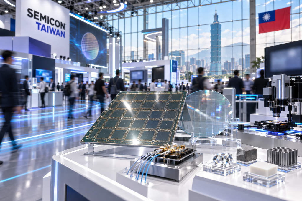
Global technology companies are pouring more resources into AI and dedicated hardware, putting pressure on the traditional consumer electronics supply chain. In semiconductors, the push to meet tighter performance and power targets is driving upgrades across materials, advanced packaging and precision equipment.
In a podcast recorded after SEMICON Taiwan, Statementdog focused on foundry order spillover, fan-out panel-level packaging, or FOPLP, diamond and silicon carbide thermal materials, and optical alignment for co-packaged optics, or CPO. The program described those technologies as core drivers for the next phase of semiconductor growth.
Advanced packaging is spreading beyond foundries
CoWoS and other 2.5D/3D packaging technologies were previously concentrated at wafer foundries. As end-market chip demand becomes more diverse, outsourced semiconductor assembly and test companies, or OSATs, including ASE (3711), SPIL and Powertech (6239), as well as European manufacturers, are moving more aggressively into advanced packaging.
Statementdog said many OSAT companies have lifted capital spending by more than 100% as they try to copy and optimize advanced packaging flows while moving up the learning curve. That, in turn, is driving a fresh wave of orders for equipment suppliers in Taiwan and overseas.
The podcast also said Taiwan Semiconductor Manufacturing Co. is expected to introduce ASML’s High-NA EUV tools around 2030. Statementdog framed that as part of TSMC’s strategy of delaying the adoption of mature specifications in pursuit of what it called the best cost efficiency.
Thermal management is opening new material paths
Higher-power chips are pushing conventional cooling structures toward their limits. Double-sided water cooling plates and new thermal interface materials are drawing more attention. Diamond, which the program described as a key fourth-generation semiconductor material, has already entered the research and development stage because of its strong heat conductivity.
Still, synthetic diamond produced through MPCVD faces several hurdles, including relatively small substrate sizes, high cost and challenges in metal bonding and processing.
Insulating silicon carbide is emerging as another route. Statementdog said it is already being used in optical waveguides and carrier wafers for thermal management. Coherent (COHR) displayed a 12-inch SiC wafer, a sign that larger-scale adoption may be getting closer.
For packaging issues such as chip shift or photolithography misalignment, the program said high-precision direct-write and inkjet coating technologies can accurately deposit dielectric materials or thermal paste and serve as an efficient correction method.
FOPLP and glass substrates are moving closer to commercial use
With wafer-level packaging, or WLP, capacity staying tight and prices moving up, FOPLP is gradually shifting from concept to actual mass-production planning. The podcast linked part of that momentum to demand for 800V SiC power device modules, including PMIC and RFIC applications, where panel-level packaging offers better area utilization.
Glass substrates are another focal point in the technology roadmap. According to Statementdog, bringing glass substrates into the stack could further increase package size and allow chips to integrate more high-bandwidth memory, or HBM, and optical engines.
Silicon photonics and CPO raise the bar for alignment tools
CPO comes with high technical barriers, especially in high-power lasers and micron-level optical alignment. Because alignment speed and precision directly affect throughput and yield, equipment makers are developing multi-axis alignment platforms, including Stewart platforms, and pairing them with piezoelectric motors or linear motors to improve performance at the micron scale.
That makes equipment capability a central competitive factor as silicon photonics and CPO advance.
Five equipment and materials areas Statementdog is watching
The podcast highlighted five parts of the supply chain that it sees as promising:
- Spillover from European capacity expansion: European OSATs and international automotive semiconductor companies are accelerating advanced packaging buildouts, with related equipment orders flowing to suppliers that offer cost advantages and production flexibility.
- Thermal materials remain unstandardized: Diamond heat spreaders, insulating SiC carriers, liquid indium metal and inkjet-applied thermal adhesives are all being explored, and no single standard has emerged.
- FOPLP is splitting into coarse and fine line-width routes: Traditional FOPLP is geared toward coarse line widths and fits power devices such as PMICs and RFICs, while chip-last and fine line-width processes are moving toward high-end logic chips, creating separate demand for dicing, etching and cleaning tools.
- High-priced opportunities in optical alignment platforms: Silicon photonics and CPO are not yet standardized in production, leaving room for expensive multi-axis precision alignment systems with higher margins.
- Equipment demand tied to glass-based packaging: As the industry shifts from glass carriers to glass substrates and interposers, demand is rising for glass cutting, drilling, slotting and backend repair equipment.
The article was first published by ABMedia and centered on how post-SEMICON Taiwan discussions are increasingly focused on FOPLP, glass substrates and silicon photonics as new commercial openings for semiconductor equipment and materials suppliers.