
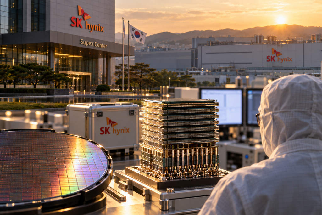
According to ChainCatcher, SK Hynix said on Sept. 9 that foundry processes can be used in the development of next-generation 3D DRAM semiconductors.
The comment came a day after the company held its 2026 SK Hynix Future Forum at the Supex Center in its Icheon complex. At the event, Vice Presidents Kim Kyung-hoon and Son Ho-young presented the main technical directions for 3D DRAM, including the use of logic foundry processes for DRAM peripheral circuits, maximizing data bus bandwidth, and ultra-short-distance transmission.
What SK Hynix highlighted for 3D DRAM
3D DRAM refers to a next-generation DRAM structure that improves integration density by vertically stacking memory cells that had previously been arranged on a flat plane. The two executives said that beyond design and thermal issues, the technology will also require solutions to packaging challenges including fine interconnects, bonding, and process integration.
They added that as the boundaries between front-end and back-end packaging, and between foundry and memory technologies, move closer together, cross-domain co-optimization will become more important.
Forum remarks on industry direction
Son said 3D technology is changing the technical boundary between wafer fabrication and packaging, and that the industry needs to build optimization methods and a new collaboration system that go beyond existing domains alongside innovation in advanced packaging.
Speaking on the same theme, Korea University professor Shin Chang-hwan said 3D DRAM is not only about vertically stacking chips but also about breaking the boundary between memory and logic. As device scaling nears its limit and data movement between systems and memory increases both latency and power consumption, a shift toward 3D technology is unavoidable, he said. Shin also proposed a 3D integration design framework linking materials, devices, packaging, and architecture through artificial intelligence.
Message from the company president
In his remarks, SK Hynix President Kwak Noh-jung said the memory market used to resemble a straight road where the goal was simply to run faster, but now looks more like a constantly changing curve. He said that beyond internal capabilities, it is also important to grasp the speed and direction of changes in the external environment and adapt flexibly.