
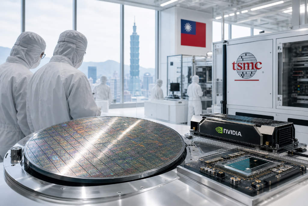
TSMC has successfully developed and validated its A16 process platform with a Super Power Rail, or SPR, backside power delivery network, according to a report by South Korean media outlet ETNews. The report said TSMC is the first foundry to implement backside power supply technology, or BSPDN, at the Angstrom-class node while fully preserving compatibility with existing design ecosystems. It added that the platform has already won support from the market’s largest AI chip customer, with NVIDIA confirming A16 for its next-generation Feynman AI accelerator platform.

Why backside power delivery matters below 2 nm
ETNews said that as semiconductor manufacturing moves into the Angstrom era, meaning below 2 nm, the conventional chip layout that places both power routing and signal routing on the front side is running into physical limits. In that arrangement, the two routing layers compete for the same constrained space, creating routing congestion and higher interconnect resistance, which can trigger voltage drops and hurt both performance stability and power efficiency.
BSPDN is meant to solve that by moving power delivery to the back of the chip and reserving the front side for signal transmission. The problem, the report said, is that conventional implementations often require changes to transistor placement or cell architecture, forcing customers to rebuild parts of their cell libraries and design tool flows. That raises adoption costs and can stretch out the early yield ramp in mass production.
According to the report, TSMC’s A16 platform stands out because it avoids both of those costs at the same time.
How SPR is positioned on A16
TSMC’s SPR approach moves the power path entirely to the backside of the chip and uses dedicated backside contacts, identified as VB, to deliver power directly to the source and drain of each transistor. That creates a full separation between power and signal paths.
The report said the main advantage is that front-side gate structures, cell dimensions, and layout area stay almost unchanged through the transition. As a result, A16 keeps the gate density of N2P and the design flexibility of NanoFlex. For large customers such as NVIDIA and Apple, which already have deep design resources tied into the N2 and N2P ecosystem, the shift to A16 would require little to no rewriting of existing cell libraries or design flows while still giving access to the gains from backside power delivery.
ETNews said that compared with N2P, A16 can raise computing speed by 8% to 10% at the same power, or reduce power consumption by 15% to 20% at the same speed. Chip density also improves by 8% to 10%. The report framed that combination as commercially attractive for AI accelerator and HPC chip designers that need both high compute throughput and strict power ceilings.
Intel and Samsung face design and timing challenges
The report contrasted TSMC’s path with Intel’s BSPDN efforts. During validation of Intel’s PowerVia technology, ETNews said, the company has had to adjust pin counts, loosen metal pitch, and redesign cell architecture, leaving a break in the design ecosystem difficult to avoid.
It also said Intel’s later 14A2 process, which targets a 21 nm line width, has run into physical bottlenecks. That has pushed Intel to evaluate a dual-sided hybrid architecture using both front-side and backside power paths. ETNews said the yield risk from that stack is higher than TSMC’s single BSPDN route.
On manufacturing schedules, the report said Intel 14A may enter limited production in 2028 at the earliest and scale in 2029. TSMC’s A16, by contrast, is set to start mass production in the fourth quarter of this year, putting the gap at at least three years. Samsung Electronics plans to introduce BSPDN on its SF2 process as well, but the report said industry assessments see its route as similar to Intel’s, with the same need to rebuild parts of the design ecosystem.
NVIDIA’s Feynman platform is set to use A16
TSMC’s technical lead has also translated into customer backing, according to the report. NVIDIA’s next-generation AI accelerator platform, Feynman, is expected to use TSMC A16 and will also mark the first large-scale deployment of CPO and SoIC 3D stacking on the platform, with mass production targeted for the second half of 2028.
ETNews said that while the industry is still evaluating BSPDN approaches from different chipmakers, NVIDIA, a long-term TSMC partner, has already made its choice. The report presented that as a strong market endorsement for A16.
The contest is now about process and ecosystem together
ETNews cited industry views saying that competition in the Angstrom era has moved beyond a simple race over transistor density. It is now a two-track contest between process capability and the depth of the design ecosystem. In that reading, A16’s advantage is not only that TSMC is first to push BSPDN toward mass production, but that it can do so with almost no design changes for customers already operating inside a mature ecosystem.
With Intel and Samsung still dealing with route selection and yield maintenance, the report said TSMC’s lead is no longer just a gap in technical metrics. It has become an ecosystem advantage as well.