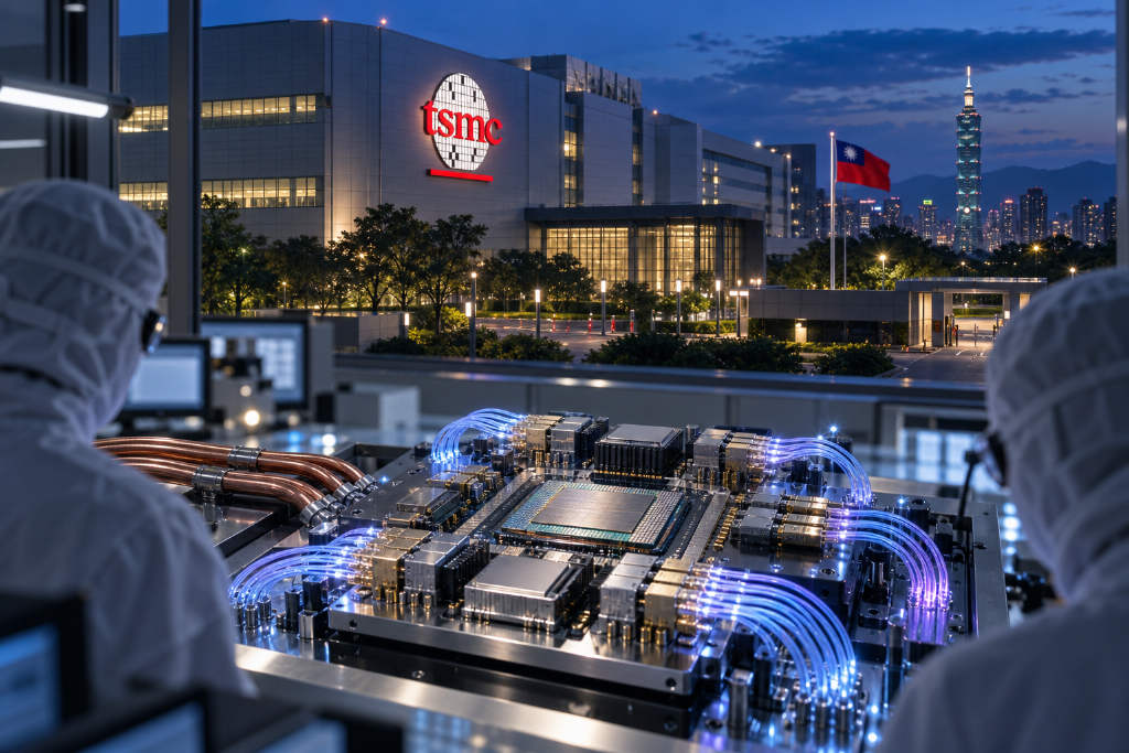
TSMC is accelerating its push into co-packaged optics, or CPO, as rising GPU and ASIC compute capacity pushes traditional copper interconnects closer to their limits in power consumption and signal transmission, according to a Sept. 14 report by Taiwan's Commercial Times cited by ChainCatcher. Industry observers say CPO bandwidth could form an "optical Moore's Law" for the AI era if it continues doubling every two years.
The report outlined three main upgrade paths for CPO bandwidth: increasing single-lane speed from 200G to above 400G, expanding optical channel counts from 16 to 32 and then beyond 64, and adopting wavelength division multiplexing, or WDM. On that basis, the theoretical ceiling by 2040 could reach about 128 times current levels. Using the present 3.2T class as a reference point, the long-term trajectory could extend into the hundreds of terabits.
TSMC's role in optical interconnects is also expanding from pure wafer foundry work to system integration across 3DFabric, CoWoS, SoIC, silicon photonics and CPO, combining compute, HBM memory and high-speed I/O. The report added that once electrical signals exceed 200G, attenuation worsens across longer copper paths including ABF substrates, PCBs and connectors, pushing the industry toward shorter copper links and longer optical links. Mass production of CPO still faces packaging, optical coupling and testing hurdles.
TSMC is accelerating its buildout in co-packaged optics, or CPO, as rising GPU and ASIC compute performance pushes traditional copper interconnects closer to their limits in power consumption and signal transmission, according to a Sept. 14 report by Taiwan's Commercial Times cited by ChainCatcher.
Industry participants said that if CPO bandwidth keeps doubling every two years, the AI era could see what they described as a "CPO Moore's Law." They pointed to three main paths for bandwidth upgrades: raising single-lane speed from 200G to above 400G, increasing optical channel counts from 16 to 32 and then beyond 64, and introducing wavelength division multiplexing, or WDM.
On that basis, the theoretical level by 2040 could reach roughly 128 times the current stage. Using today's roughly 3.2T class as a baseline, the longer-term ceiling could move into the hundreds of terabits.
TSMC's role in optical interconnects is extending from wafer foundry manufacturing into system integration. The report said that spans 3DFabric, CoWoS, SoIC, silicon photonics and CPO, with the company gradually integrating compute, HBM memory and high-speed I/O.
Once high-speed electrical signals move above 200G, signal attenuation becomes more severe after traveling through longer copper paths such as ABF substrates, PCBs and connectors, the report said. That shift is steering the industry toward shorter copper paths and longer optical paths.
In packaging architecture, optical engines are currently being placed on the substrate first. The next step could move CPO onto the interposer. Over a longer horizon, SoIC could enable 3D vertical integration between photonic integrated circuits, or PICs, and ASICs.
Industry sources added that CPO still needs to clear packaging, optical coupling and testing challenges before reaching mass production.
This article was originally published by Bit.Fan. For more cryptocurrency news and market insights, visit www.bit.fan. Disclaimer:
The market information, project data, and third-party content displayed on this platform are for industry information sharing only and do not constitute any form of investment advice or return commitment.
Cryptocurrency trading carries high risks. Users should fully assess their risk tolerance and make independent decisions. All profits, losses, and legal responsibilities are borne by the users themselves.