
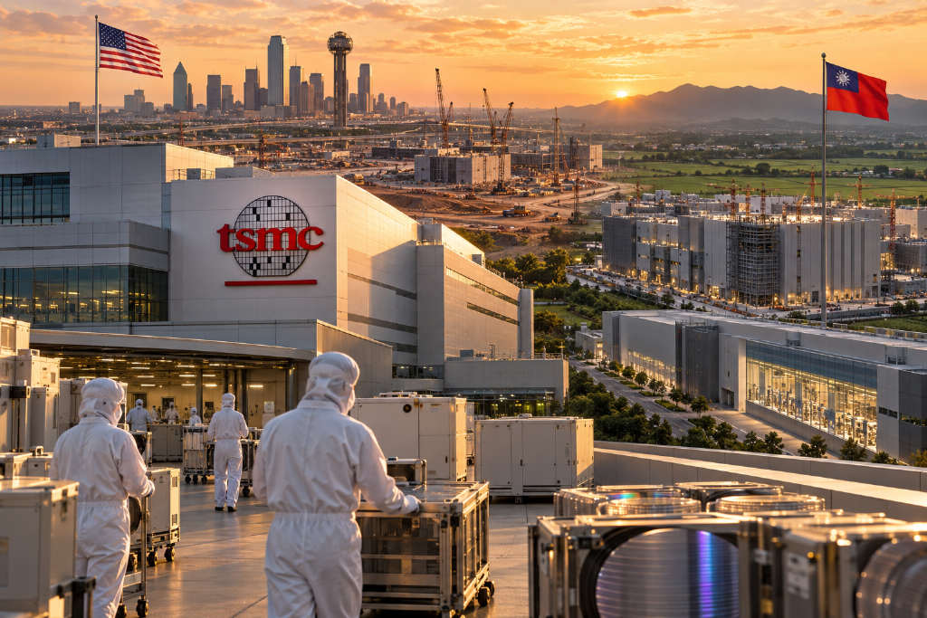
Taiwan Semiconductor Manufacturing Co. is evaluating a second major manufacturing campus in the U.S. and is also considering a fresh expansion of advanced packaging capacity in Taiwan, according to the source report.
Counterpoint Research said TSMC held a 71% share of the pure-play foundry market in the second quarter this year, widening the gap with rivals. The research firm attributed that growth to the start of 2 nm mass production, continued 3 nm capacity ramp-up, and tight supply in 8-inch, 12-inch and advanced packaging capacity, factors that strengthened TSMC’s pricing power and improved revenue visibility.
A second U.S. campus is under evaluation
Citing recent information from the semiconductor equipment supply chain carried by Taiwanese media, the report said TSMC is assessing a second large manufacturing park in the U.S. after Arizona. The plan under discussion involves six additional advanced wafer fabs, with Dallas and North Texas identified as possible sites. If the project moves ahead, TSMC would have two advanced manufacturing bases in the U.S., one in Arizona and another in Texas.
TSMC has not formally responded to the report. Talk of a new Texas fab has been circulating in the semiconductor supply chain, and several suppliers said they had heard related discussions. Even so, TSMC has not formally asked suppliers to prepare in advance for plant construction, leaving the plan subject to change.
The report said one of the main drivers behind a broader U.S. footprint is continuing demand for artificial intelligence and high-performance computing, or HPC. TSMC’s manufacturing base in Phoenix, Arizona, has already raised its total planned investment to about $265 billion, with plans for six wafer fabs, two advanced packaging facilities and one R&D center. The stated goal is a full manufacturing cluster spanning wafer fabrication, advanced packaging and research.
As AI accelerators improve, leading-edge process technology is no longer the only critical factor. Advanced packaging such as CoWoS in 2.5D and 3D forms, along with technologies tied to HBM, is gaining weight in the supply chain. For AI chip customers such as Nvidia and AMD, wafer fabrication, advanced packaging and high-bandwidth memory need to work more closely together. That is why the report said TSMC is extending advanced packaging capabilities in the U.S. while building advanced wafer fabs there.
The U.S. customer base is another reason for local expansion. Apple, Nvidia, AMD and Qualcomm are among TSMC’s major customers, and the push to localize advanced chip manufacturing in the U.S. has increased demand for domestic production capacity. The report also pointed to uncertainty in U.S. trade and tariff policy as a factor pushing TSMC closer to customers and end markets.
Dallas and North Texas named as potential locations
Dallas and North Texas were described as strong candidates because of their semiconductor base. The area has long been known as the “Silicon Prairie” and already hosts clusters in wafer manufacturing, semiconductor equipment, materials, optical communications and electronics manufacturing. Texas Instruments has a large manufacturing base there, while Samsung operates wafer fabrication capacity in Austin. The broader region also includes many electronics, communications and technology companies.
Energy, land and labor are part of the appeal. Advanced wafer fabs require heavy electricity and water use, along with sizable industrial land and a skilled workforce. As AI data centers expand quickly, power and infrastructure pressure has been rising in parts of the U.S., making energy supply an increasingly important site-selection factor for advanced fabs.
By contrast, TSMC’s Arizona base has faced challenges in construction costs, labor and utilities infrastructure in recent years. The report said Texas stands out in land, energy and industrial talent, making it a key candidate as TSMC studies a second U.S. campus.
If TSMC ultimately launches that second U.S. park, the total investment could exceed the current Arizona plan of about $265 billion, because later fabs may use more advanced process nodes and may be paired with advanced packaging and research facilities.
For now, the six-fab plan, the investment amount and the process nodes have not been officially confirmed by TSMC. Supply-chain sources cited in the report said Dallas and North Texas may already be in the later stage of site evaluation, but a final decision would still need board approval.
If the plan is approved, TSMC’s U.S. presence would begin shifting from a single manufacturing base to a regional industrial layout. Arizona would continue to focus on advanced wafer fabrication and advanced packaging, while Texas would build another manufacturing core on top of the local semiconductor and industrial ecosystem. The report said that could also move the U.S. advanced semiconductor supply chain from isolated fab projects toward a more clustered model.
Five more advanced packaging plants are being assessed in Chiayi
At the same time, TSMC is said to be weighing a further expansion of advanced packaging in Taiwan. With AI chip demand still rising, advanced packaging has become the next major area of semiconductor capacity expansion after leading-edge process technology. Supply-chain information cited in the report said TSMC is evaluating five additional advanced packaging plants in Phase 3 of the Chiayi Science Park project.
If that plan is carried out, the number of advanced packaging plants planned in Chiayi would rise from five to ten, expanding the local AI packaging cluster.
On Sept. 23, Taiwan authorities announced the information disclosure and public comment process for the “Chiayi Park Expansion Plan (Phase 2 Expansion),” which the market has referred to as “Chiayi Phase 3.” According to the plan, the expansion would cover artificial intelligence, heterogeneous packaging, silicon photonics, high-speed broadband networks, quantum technology and net-zero related development. The project still needs environmental review and later approval and has not been finalized.
According to data from the Southern Taiwan Science Park Bureau cited in the report, TSMC has already planned two advanced packaging plants, P1 and P2, in Phase 1 of the Chiayi park, with mass production expected in 2027. Phase 2 includes three plants, P3, P4 and P5, and P3 has already started construction. Phase 2 is expected to complete development in 2031. Recent supply-chain talk says TSMC is now evaluating another five advanced packaging plants in Phase 3 as AI chip orders keep rising, though the company has not confirmed investment size or product planning.
CoWoS and 3D packaging remain at the center of the buildout
The report tied this expansion directly to rapid growth in demand for advanced packaging such as CoWoS. Compared with traditional packaging, CoWoS uses a silicon interposer to integrate GPUs, CPUs, HBM and I/O chiplets into one package. That allows higher interconnect density and bandwidth while lowering data-transfer latency and power use between chips. GPUs paired with HBM have become the mainstream architecture for AI accelerators, and the combination of more HBM stacks and larger chip sizes has turned advanced packaging into a major capacity bottleneck.
TSMC’s advanced packaging program has been in place for more than a decade. The company began mass production of CoWoS in 2012, initially for FPGAs, networking chips and high-performance computing products. As generative AI drove a jump in GPU and HBM demand, the importance of CoWoS increased sharply, and TSMC kept adding capacity and upgrading packaging technology.
CoWoS has evolved toward larger package sizes. TSMC has developed CoWoS-S, CoWoS-R and CoWoS-L. The report said CoWoS-L combines redistribution layers with local silicon interconnect, allowing it to move past the size limits of conventional silicon interposers and making it better suited for large AI chips and multi-die systems.
TSMC is also advancing 3D packaging technologies such as SoIC. Through hybrid bonding, SoIC enables vertical stacking of chiplets. TSMC has folded CoWoS, SoIC and related technologies into its 3DFabric platform as the basis for future chiplet and heterogeneous integration.
Chiayi and Kaohsiung are part of a broader southern Taiwan buildout
The report said silicon photonics is also a key development area in the Chiayi expansion. As AI data-center networks move toward 1.6T, 3.2T and higher speeds, conventional electrical interconnects are facing pressure in both power consumption and bandwidth. That is raising the importance of silicon photonics and co-packaged optics. In that view, competition in AI chips may extend beyond high-speed links between GPUs and HBM to optical interconnects between chips and networks.
At the same time, the Qiaotou Baipu Industrial Park in Kaohsiung has already started development. It is positioned as a cluster for advanced semiconductor packaging materials and equipment supply chains, along with an AI advanced manufacturing base and testing and validation sites for equipment and materials. The park covers about 88.73 hectares. It is expected to open land leasing for plant construction in the first quarter of 2027 and complete standard factory buildings in the second quarter of 2029.
From Chiayi to Kaohsiung, southern Taiwan is building a supply chain around AI chips that spans advanced manufacturing, packaging, equipment and materials. For TSMC, the Chiayi expansion is not only an extension of CoWoS capacity. The report said it also creates manufacturing space for larger package sizes, HBM4, chiplets and future optoelectronic integrated packaging.
AI demand is driving parallel expansion in wafer fabs and packaging
The source article said TSMC’s continued expansion in both wafer fabrication and advanced packaging reflects a shift in the logic of semiconductor manufacturing under AI demand. As demand grows for GPUs, HBM, chiplets and high-speed interconnects, the importance of both leading-edge process nodes and advanced packaging is increasing at the same time. In that framework, chip competition is no longer only about process nodes, but also about the combined strength of wafer manufacturing, advanced packaging, memory and interconnects.
The original article was from the WeChat account “半导体行业观察” (ID: icbank) and was credited to its editorial team.