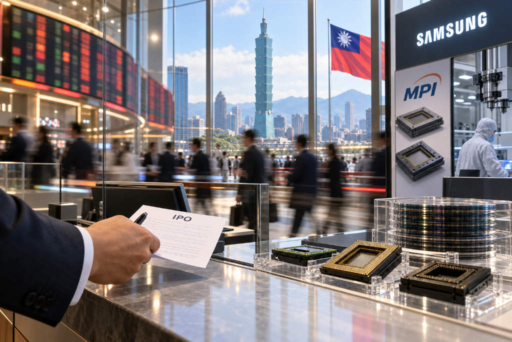
Hance2026-09-09 00:28:46Hance IPO pricing gap lifts attention on semiconductor test names Yingwei and MPIHance (7856), a key stock on Taiwan’s emerging market, is scheduled to begin its initial over-the-counter public subscription on Sept. 10, with an underwriting price set at TWD 2,250 per share. The price marks a record high for Taiwan’s primary listing and OTC underwriting market. Based on an emerging-market trading price of about TWD 4,700 cited in the source, the implied spread for one standard lot exceeds TWD 2.4 million, drawing strong market attention. The valuation gap has also pushed investors to revisit pricing across semiconductor testing interface and inspection equipment names. The report said stocks such as Yingwei (6515) and MPI (6223) posted notable market reactions as capital rotated into higher-priced semiconductor inspection plays. Yingwei hit limit-up during a broader market pullback, while MPI drew added attention after the source linked the company to a TSMC-certified testing equipment supply chain adopted by Samsung Electronics for its silicon photonics push. ABMedia also tied the move to demand from more advanced semiconductor manufacturing, including angstrom-level processes, heterogeneous integration, EUV, and silicon photonics, all of which raise the technical bar for inspection equipment and probe cards.1210
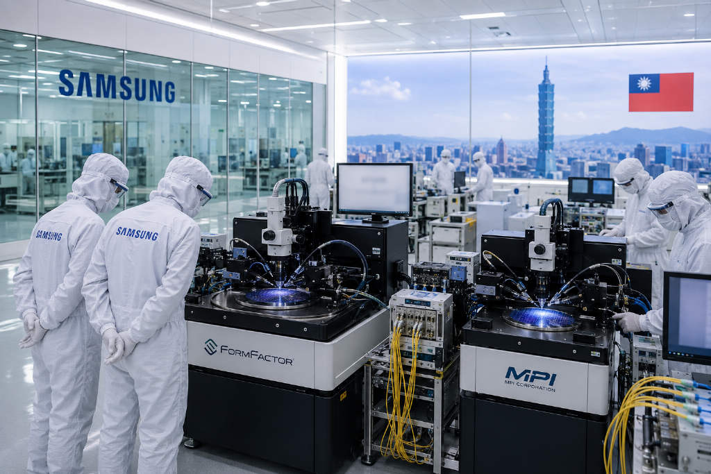
Samsung Elect2026-09-07 10:37:10Samsung adopts the same photonic chip testing platform used by TSMC, targets in-house PIC evaluation this yearSamsung Electronics is using probe stations from U.S.-based FormFactor and Taiwan-based MPI to test silicon photonic integrated circuit, or PIC, wafers, according to a report by Korean semiconductor outlet The Elec cited by BlockBeats on Sept. 7. The company aims to complete its own internal PIC evaluation within the year. The report said both FormFactor and MPI have already passed equipment verification tied to Taiwan Semiconductor Manufacturing Co.'s co-packaged optics, or CPO, and silicon photonics testing workflows. Samsung is using the same basic testing setup to examine optoelectronic properties of PIC wafers across wavelength and frequency domains, checking whether optical devices perform signal transmission and electro-optic conversion as intended. Samsung had previously relied on outside institutions including Belgium-based imec for PIC wafer verification. It is now building its own testing environment and conducting repeat evaluations. The company is also preparing customer evaluations and has said related projects will enter mass production starting in the second half of this year. The report added that Samsung plans to launch silicon photonics foundry services in 2027, offering optical device process technology, device libraries and PDKs, while also developing optical engines that combine EIC and PIC for future CPO use in products beyond network switches, including GPUs and CPUs.1530