


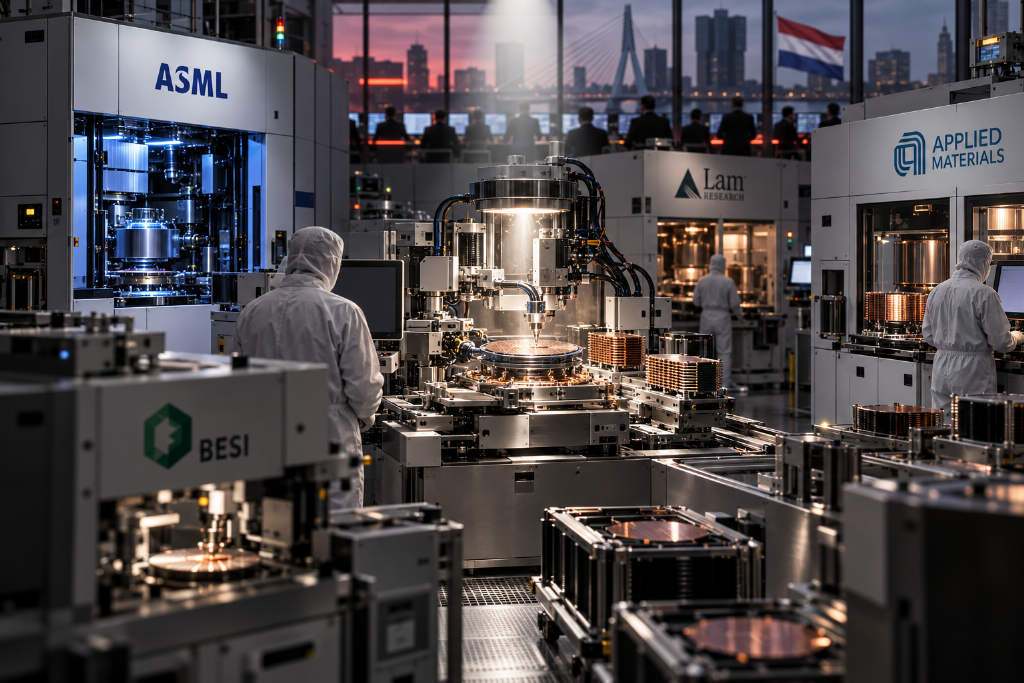
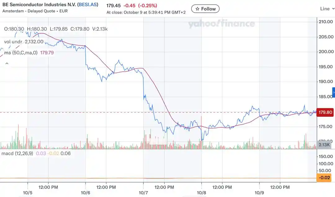
A new fight is taking shape in semiconductor equipment, and advanced packaging is at the center of it. In early October, Bank of America downgraded Dutch packaging equipment maker Besi on concerns that ASML could move into the hybrid bonding equipment market and that demand for HBM-related tools may be delayed. Besi shares fell 5.39% on Oct. 6. A day later, after UBS also cut its rating, the stock dropped another 8.49%, bringing the two-day decline to about 13.4%.
ASML had already delivered its TWINSCAN XT:260 lithography system for advanced packaging in 2025, and reports this year said it is developing hybrid bonding equipment, extending its reach beyond its traditional lithography business.
The selloff in Besi shares has put the competitive landscape in advanced packaging equipment back in focus.
Front-end equipment leaders are moving into advanced packaging
Applied Materials and Lam Research are also accelerating their efforts. In the first week of October alone, Applied Materials announced expanded cooperation with Besi and Intel, with work spanning hybrid bonding, thermocompression bonding, chip-to-panel technologies and Foveros 3D packaging. Lam Research has continued to broaden its equipment footprint in TSV and 3D interconnects through etch, deposition and copper electroplating. Reuters reported in March that both Lam Research and Applied Materials had shown interest in acquiring Besi.
The three front-end equipment giants — Applied Materials, Lam Research and ASML — are entering advanced packaging through different technical paths. At the same time, established packaging equipment leaders are becoming targets for partnerships, investment and possible acquisitions. The once clearer division between front-end and back-end equipment is starting to shift, with advanced packaging emerging as a new competitive arena.
Applied Materials: building a broader process chain with Besi
Applied Materials has been working on advanced packaging for years. Back in 2020, it set up a joint R&D program with Besi in Singapore, combining its own capabilities in etch, planarization, thin-film deposition, wafer cleaning, metrology and particle control with Besi’s strengths in precision die placement, interconnect and assembly.
A key result of that work is the Kinex integrated die-to-wafer hybrid bonding system. Unlike traditional packaging tools that focus mainly on die placement and connection, Kinex is designed to integrate pre-bond surface treatment, cleaning, activation and alignment into a tighter manufacturing flow.
That design reflects the demands of hybrid bonding itself. The two chips or wafers being joined must not only achieve very high geometric alignment accuracy, but also maintain surface flatness, cleanliness and stable material conditions. Even if the bonder has strong positioning accuracy, defects can still appear if earlier steps introduce particle contamination, abnormal copper pad recess or unstable surface conditions. The logic behind the Applied Materials-Besi partnership is to combine front-end materials engineering with back-end precision assembly to improve final yield through cross-process coordination.
Applied Materials has not limited itself to Besi. It has also worked with Austrian wafer bonding equipment maker EV Group, or EVG, on wafer-to-wafer bonding solutions.
On Oct. 1, Applied Materials and Besi expanded their cooperation again. According to the official announcement, Besi will become an innovation partner at Applied Materials’ EPIC R&D center in Silicon Valley. The two companies will continue work on die-to-wafer hybrid bonding and jointly study TCB scaling, chip-to-chip, chip-to-panel and new integration architectures for optical interconnects. The EPIC center has a planned investment of as much as $5 billion, with spending to be rolled out alongside customer projects. One of its stated goals is to bring chipmakers, equipment suppliers and materials companies into joint development earlier, shortening the path from lab work to volume production.
At the industry level, that points to an effort by Applied Materials to pull advanced packaging out of a relatively standalone back-end role and into a broader materials engineering framework.
Five days later, Applied Materials also announced deeper cooperation with Intel, extending joint R&D to next-generation transistors, on-chip interconnects and Foveros 3D advanced packaging.
Those two partnerships involve different counterparties, but the technical logic overlaps. In 3D stacking, interconnect density, power delivery, thermal structures and material stress all affect one another. Performance gains in next-generation chips are becoming harder to achieve through only one layer of the stack, whether that is process technology, metal interconnect or packaging.
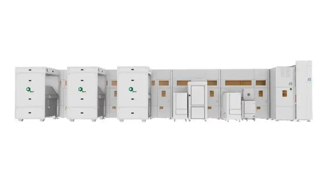
Applied Materials executive Prabu Raja framed it this way: advanced packaging is no longer just physical assembly at the back end, but a materials engineering shift that requires wafer-level precision and cleanliness.
Lam Research: extending from etch and deposition into 3D interconnects
Lam Research is taking a different route. Its push into advanced packaging leans more heavily on process equipment strengths it already built in logic, DRAM and 3D NAND manufacturing, especially in high-aspect-ratio etch, thin-film deposition and metal interconnect.
As advanced packaging moves deeper into 3D structures, those technologies are finding more use cases. In stacked chips, through-silicon vias, or TSVs, provide vertical electrical connections between layers. Making deep, narrow vias in silicon requires high-aspect-ratio etch while maintaining sidewall shape, etch uniformity and defect control.
Lam Research’s Syndion deep reactive ion etch system targets deep-etch applications including TSVs. But etching the via is only the first step. After the insulating layer, barrier layer and seed layer are formed, the via still has to be filled with metal to create a reliable electrical path. Voids, seams or other defects during copper fill can affect resistance, heat dissipation and long-term reliability.
In July, Lam Research highlighted its SABRE 3D copper plating platform, which is aimed at the manufacturing demands of complex metal interconnects in advanced packaging. The company said that as interconnect structures become finer, requirements for fill uniformity and void control keep rising. SABRE 3D uses electrochemical deposition to provide metal fill for TSVs, wafer-level packaging and redistribution layers.
Lam Research has also deployed the VECTOR TEOS 3D dielectric deposition system, along with related wet and deposition processes for large-format substrates.
For Lam Research, the attraction of advanced packaging goes beyond hybrid bonding itself. From conventional 2.5D packaging to 3D chip stacking and panel-level packaging, more manufacturing steps now require precise etch, thin-film deposition and metal interconnect processes. Those are all areas where the company already has a long operating history.
That means Lam Research does not necessarily need to replace Besi in bonding tools directly. It can also expand the range of critical process equipment it supplies and capture more value across the advanced packaging chain.
Still, its interest in bonding equipment is notable. In March 2026, Reuters, citing people familiar with the matter, reported that Besi had drawn takeover interest because of its hybrid bonding technology, and that Lam Research and Applied Materials were among the names involved.
So far, public reporting has not confirmed that any such deal was completed. Even so, the episode suggests that the next phase of competition in advanced packaging equipment may involve not only product development and process advances, but also equity investment, strategic partnerships and industry consolidation.
ASML: from lithography to hybrid bonding
ASML’s possible move is different again, and potentially more direct for the traditional hybrid bonding equipment market.
As the sole supplier of EUV lithography systems, ASML’s core strengths lie in high-precision optics, motion control, wafer positioning, deformation compensation and nanometer-scale overlay accuracy. Those capabilities were built for transferring ever-smaller circuit patterns onto wafers, but hybrid bonding also depends on a closely related challenge: aligning metal interconnect structures on two wafers or chips with extreme precision and keeping that alignment stable during bonding. That creates a clear technical overlap between ASML’s existing expertise and hybrid bonding equipment.
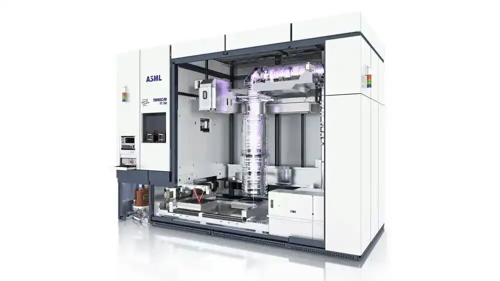
ASML has already entered advanced packaging through dedicated lithography tools. At its annual general meeting in April 2026, the company said it had delivered the first TWINSCAN XT:260 i-line lithography system for 3D integration and advanced packaging applications. Unlike EUV systems used mainly in advanced logic manufacturing, the XT:260 is aimed at specialized patterning needs in advanced packaging. ASML said in presentation materials that micro-bump processes require greater depth of focus, while hybrid bonding places higher demands on pattern resolution. As interconnect density in advanced packaging rises, lithography itself is becoming a more important factor in packaging technology development.
The TWINSCAN XT:260 introduced last year is an i-line scanner capable of processing 270 wafers per hour. According to the source article, ASML plans over the next 10 to 15 years to shift more of its business focus from pure front-end chip production equipment toward packaging and bonding technologies as demand for AI chips grows.
But ASML does not appear content to stop at packaging lithography. In March, Korean media outlet The Elec reported that ASML had started overall architecture design for hybrid bonding equipment and had been in contact with long-time suppliers including Prodrive Technologies and VDL ETG. Those companies have previously supplied precision motion systems, drive units and mechanical structures for ASML lithography tools. If ASML transfers its experience in high-precision motion platforms into bonding tools, the technical gap between lithography systems and hybrid bonding equipment could narrow further.
ASML has also disclosed related patents. International patent WO2026098870A1, published on May 15, 2026 and titled Bonding Apparatus, lists ASML Netherlands BV as the applicant. The patent covers a bonding device for two semiconductor substrates and focuses on improving alignment issues during bonding by controlling the condition of the substrate support surface. The filing says internal wafer stress, support surface condition and flatness can all cause alignment deviation during bonding. That has an obvious connection to ASML’s long-running work in wafer deformation compensation, position measurement and precision motion control.
A patent filing, of course, does not mean a production-ready tool already exists. ASML has not publicly confirmed a commercial delivery timeline, customer qualification progress or volume manufacturing performance for any hybrid bonding system. Even so, the possibility of new competition is already affecting expectations for traditional equipment suppliers. When Bank of America downgraded Besi on Oct. 6, it specifically cited the risk that ASML could enter the hybrid bonding market.
For Besi, that risk is meaningful. Besi’s position in advanced packaging equipment has been built on long experience in precision die placement, assembly processes and hybrid bonding technology. If ASML enters formally, it could bring a new competitive force based on nanometer-scale positioning, precision metrology and large-scale complex system engineering.
There is still a long path, though, between having relevant technical building blocks and delivering a commercially competitive tool that passes fab qualification for volume production. Whether ASML can truly challenge Besi will depend on alignment accuracy, throughput, yield, tool stability, cost and customer qualification progress, not on patents or supply-chain reports alone.
Why hybrid bonding has become the focal point
One reason front-end equipment makers are moving into advanced packaging is that chip interconnect technology is changing.
In traditional 2.5D and 3D packaging, chips are usually connected through micro-bumps. Thermocompression bonding, or TCB, uses heat and pressure to create reliable connections between solder and metal pads. The process is widely used in high-performance computing and memory chips. But as the number of stacked layers rises and interconnect density increases, conventional micro-bump structures face tighter requirements in pitch, connection height, parasitic effects and thermo-mechanical reliability.
Hybrid bonding offers another route. By combining direct dielectric bonding with metal interconnect, it reduces dependence on conventional solder bumps and opens the way to smaller pitch, higher connection density and more compact chip stacking.
In May 2026, Belgium-based research center Imec and EV Group said they had achieved a 200 nm copper interconnect pitch in wafer-to-wafer hybrid bonding research. The team reported post-bond copper pad overlay below 40 nm for all test chips on 300 mm wafers.
Imec also said in related research that beyond alignment accuracy, continued scaling in hybrid bonding still depends on solving issues including surface topography control from CMP, copper corrosion, dielectric reliability and metal diffusion along the bonding interface. That points to a deeper convergence between packaging steps such as placement, bonding and inspection and the materials engineering capabilities long associated with front-end wafer manufacturing.
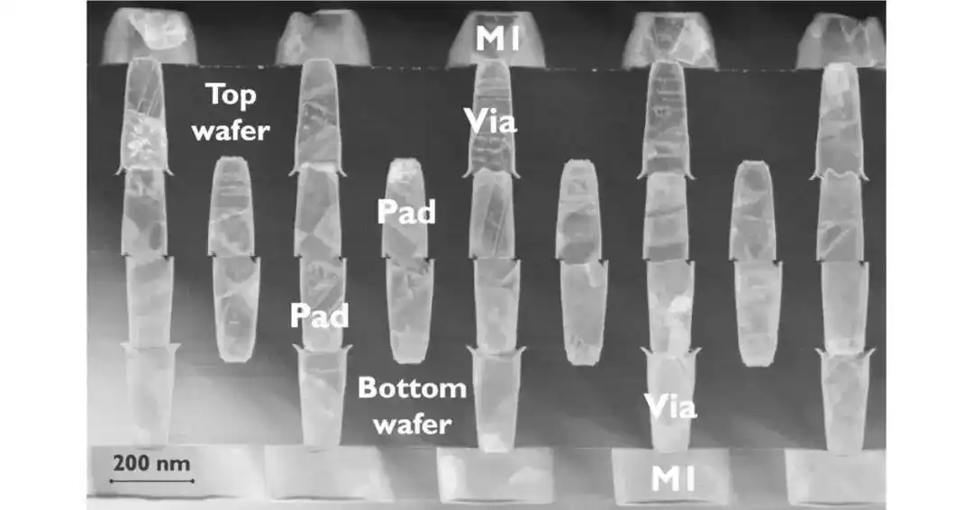
Competition in hybrid bonding equipment may therefore depend less on the bonder’s alignment accuracy and throughput alone, and more on whether the full process flow can remain stable, clean and capable of delivering controllable production yield.
Hybrid bonding is not set to replace every existing packaging technology. TCB still has a mature supply chain and production experience, and different interconnect densities, chip structures and cost targets mean the two approaches may coexist for a long time. Applied Materials’ expanded work with Besi specifically includes TCB scaling, which itself shows that the industry has not abandoned the traditional thermocompression route. The more likely outcome is a market where multiple technologies advance in parallel rather than one bonding process quickly taking over.
HBM and 3D integration will shape the next wave of tool demand
Equipment makers are investing heavily in hybrid bonding, but the pace of adoption by chipmakers will still determine the size of the market.
High-bandwidth memory, or HBM, has become one of the most closely watched applications in advanced packaging. As AI accelerators demand more memory bandwidth and capacity, HBM stacks are getting taller, and issues such as die thinning, vertical interconnect, thermal stress and package thickness are becoming more complex. Hybrid bonding could offer a new path for future HBM products through higher interconnect density and more compact connection structures.
That does not mean memory makers will switch at scale right away. For Samsung, SK hynix and Micron, the decision will depend not only on the theoretical advantages of the technology, but also on yield, capacity, equipment spending, cost and reliability in actual production. HBM is already a highly complex stacked memory product, and any added process step can change the cost structure of the entire manufacturing flow.
So it remains unclear at which HBM generation, and in which stacking architecture, TCB and hybrid bonding will begin to show a clear division of labor.
When Bank of America downgraded Besi on Oct. 6, it cited not only the potential threat from ASML but also the possibility that demand for HBM-related hybrid bonding equipment could be delayed. That captures a current tension in the market: more equipment makers want to secure a position in hybrid bonding early, but the timing of large-scale tool orders still depends on downstream technology choices and production schedules.
HBM is not the only possible demand driver. In advanced logic, Intel’s Foveros Direct and TSMC’s SoIC 3D integration technologies also rely on dense vertical interconnects to shorten data paths between chip layers.
Over a longer horizon, Imec’s CMOS 2.0 research direction is exploring how to split different functional blocks across different wafer layers and then reintegrate them through dense 3D interconnects, in an effort to move beyond the limits of conventional two-dimensional chip area and interconnect. That means future demand for hybrid bonding may expand from parts of advanced logic and memory into more complex heterogeneous integration architectures.
If those new chip architectures reach volume production, demand may spread from bonding tools alone into CMP, cleaning, thin-film deposition, metrology and precision motion control.
The competition around hybrid bonding today is, at its core, an early contest over who will shape the manufacturing stack for future 3D integration.
This article is based on a report from the WeChat public account Semiconductor Industry Observer (ID: icbank), written by Du Qin DQ.