
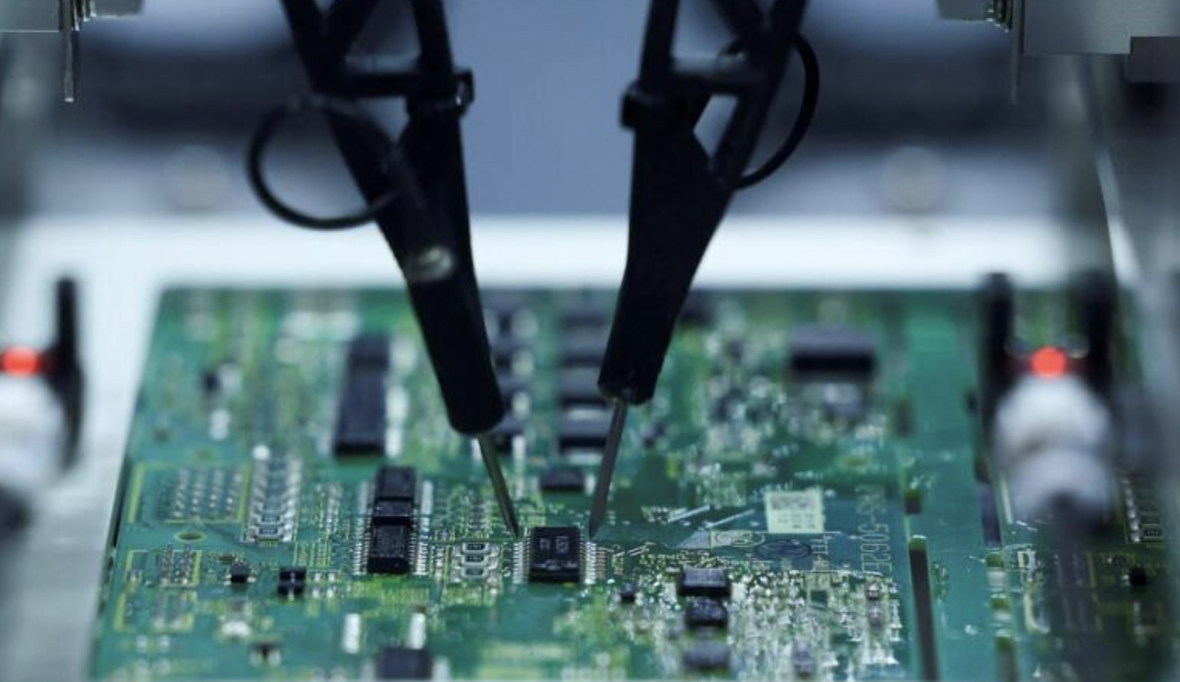
Reports that China has started small-batch production of immersion deep ultraviolet lithography tools have triggered a wave of market excitement. A PANews article says that reaction is running ahead of the facts.
Written by Hanya Hu, the piece argues that the latest development is better understood as a move from research and prototype validation into initial production and customer introduction, not as full-scale mass production and not as a sign that China has already broken ASML’s hold on high-end lithography.
According to the article, a state-backed company in Shanghai has begun small-batch production of domestic immersion DUV systems. It plans to ship about five units this year to Semiconductor Manufacturing International Corp., Hua Hong Semiconductor, and ChangXin Memory Technologies, with output targeted at roughly 20 units in 2027. Around the same time, the Shanghai Micro Electronics Equipment SSA800 series was also said to have entered full production, with an annual capacity target of 50 units. The article says these two threads are often mixed together, which can distort expectations.
What Reuters reported and what remains unproven
The article points to a July 27 Reuters report citing The Information, which said an unnamed Chinese state-backed company had started making domestic immersion DUV lithography systems. Reuters said the first batch is expected to be delivered in 2026 to SMIC, Hua Hong Semiconductor, and ChangXin Memory Technologies, with about five units planned this year and about 20 in 2027.
Reuters also said the machine still trails ASML in performance and reliability, needs more testing, and remains some distance from true large-scale commercial production. China’s EUV efforts, in the same report, were still described as being at the prototype stage.
The PANews article says these caveats matter. Its first point is that “started manufacturing and entered customer introduction” is a more accurate description than “fully mass produced.” The latter would suggest customer acceptance has already been completed and that the machines can run in fabs over long periods at stable, full-load commercial standards. Public information, the article says, does not establish that yet.
Second, numbers circulating online such as “supports 28 nm,” “more than 85% localized,” and “yield above 90%” have not been backed by full testing reports from the tool maker, customer fabs, or an authoritative third party. The article says there is still no clear statistical definition for those figures.
That matters especially for the “90% yield” claim. The article notes that the figure could mean factory acceptance yield, single-layer exposure pass rate, wafer yield, or full-chip yield. Those are very different measures. Without testing conditions, product types, wafer counts, and customer acceptance standards, the number does not have much analytical value.
This is DUV progress, not an EUV breakthrough
The article draws a clear distinction between DUV and extreme ultraviolet, or EUV, lithography. The current advance is in DUV.
Within DUV, the article lays out several categories: KrF tools using a 248 nm light source, ArF dry tools using 193 nm, and the more advanced 193 nm ArF immersion systems. Immersion lithography adds a layer of highly purified water between the projection lens and the wafer to raise numerical aperture and improve resolution. ASML’s immersion DUV systems, the piece says, are used for both mature nodes and some advanced-node production through multi-patterning.
EUV is different in kind, not just in degree. It uses 13.5 nm light, and because most materials absorb EUV radiation, those tools cannot rely on traditional lens systems. They require multilayer reflective optics in a vacuum environment. In the article’s framing, moving from DUV to EUV means a full change across the light source, reflective optics, vacuum systems, masks, photoresists, contamination control, precision stages, and overall machine control systems.
For that reason, the article says domestic immersion DUV progress mainly helps fill a domestic supply gap in advanced DUV tools. It can improve supply-chain security for mature processes and part of the advanced-process stack. It does not mean the EUV bottleneck has been solved.
Why DUV still matters in advanced manufacturing
The PANews piece says DUV and EUV will coexist in modern fabs for a long time. A chip usually contains dozens of patterned layers or more, and only a limited number of the most demanding layers need EUV. Many other layers still rely on DUV.
It cites ASML’s own description that EUV handles the most complex and critical layers in advanced chips, while a large number of remaining layers continue to use different types of DUV tools.
The article also pushes back on the idea that DUV is only for mature chips. Through double, quadruple, and more complex multi-patterning, DUV can be extended to the 7 nm class. It points to SMIC’s ability to make 7 nm-class chips without EUV equipment, relying instead on imported immersion DUV systems and complicated multi-patterning. It also notes that Taiwan Semiconductor Manufacturing Co.’s initial N7 process mainly used DUV, and that N7+, which entered volume production in 2019, was TSMC’s first process to use EUV at scale.
Still, the article says the tradeoff is harsh. As nodes advance, DUV requires more exposures, more masks, tighter overlay, and more process steps. Cycle times stretch out, defect risks rise, and manufacturing costs increase. EUV’s value is that it can cut down some of those complex DUV multi-patterning steps. The article cites ASML annual report language saying EUV can turn certain complicated multi-patterning flows into relatively simpler single-patterning steps.
Even if domestic immersion DUV systems eventually clear customer validation, the article says, the achievement would mainly answer whether China can obtain high-performance DUV equipment on its own. That may carry strategic weight for 7 nm-class production, but it does not solve the economic equation for 5 nm, 3 nm, or 2 nm manufacturing.
What five machines do and do not mean
The number five, the article says, tends to push observers into two equally flawed camps. One side dismisses it as too small to matter. The other treats any domestic buildout as proof that ASML’s monopoly has already been broken.
The article offers a rough comparison. Based on ASML annual report data, ASML recognized sales of 131 ArF immersion lithography systems in 2025. In the second quarter of 2026, ASML said its annual immersion DUV capacity for 2026 was about 130 units and that it planned to raise that by about 30% in 2027. On a simple unit basis, the five domestic systems planned this year equal about 4% of ASML’s annual immersion DUV sales.
But tool counts alone are not enough. The article says the metrics that really matter include wafer throughput per hour, overlay precision, uptime, continuous run time, defect rates, maintenance cycles, and how well the machines fit into an existing production line.
It cites publicly available parameters for one current ASML immersion DUV model, showing throughput of as much as 330 wafers per hour and matched-machine overlay of about 2.5 nm. Comparable full parameters for the domestic tool have not been publicly released.
That is why the first five units matter most as a field test in real fabs, the article argues. The key questions are whether the tools can run continuously and stably at SMIC, Hua Hong, and CXMT; whether they can work smoothly alongside etch, deposition, cleaning, inspection, and metrology tools; and whether they can win second-batch orders from customers. If any critical indicator falls short of production standards, the machines could remain stuck in trial and validation use for a long time. On that reading, five units mark the start of industrialization, not a large-scale import replacement capacity.
Why the article does not add Shanghai Micro Electronics numbers into the same bucket
The market has also circulated claims that Shanghai Micro Electronics Equipment’s SSA800 series has entered full production with annual capacity of 50 units or even 120 units. The PANews article says those figures appear in multiple versions and still lack clear company disclosures, customer acceptance reports, or fab procurement disclosures.
As of May 2025, Reuters still described Shanghai Micro Electronics’ commercially supplied front-end lithography capability as 90 nm-class in its survey of China’s semiconductor equipment sector. The article also says that while SiCarrier had applied for a number of DUV-related patents by then, it had not publicly shown a complete product.
The piece does not rule out technical progress over a year. It does say that, without new formal evidence, it is not appropriate to add rumored SSA800 output directly to the five systems in the latest report, and it is even less appropriate to conclude from that that China can already produce more than 100 immersion DUV tools a year.
For lithography tools, the article says, official launch, manufacturing completion, installation in a customer fab, fab acceptance, and stable volume production are separate stages. Blurring them together invites wrong conclusions about industrial maturity.
EUV still sits at a very different stage
On EUV, the article says China has made engineering progress but remains much farther behind. It refers to a Reuters investigation from December 2025 saying China had built a domestic EUV prototype in Shenzhen. That machine had generated extreme ultraviolet light and entered testing, but had not yet produced usable chips.
The related project proposed using a domestic prototype to produce working chips in 2028, though people close to the effort said 2030 might be more realistic. Reuters also said China continued to face significant challenges in key areas such as high-precision reflective optics.
For the PANews author, that means domestic EUV has taken an important step and engineering feasibility is being tested. But moving from “can generate EUV light” to “can stably manufacture advanced chips” still requires solving a long list of issues: source power and stability, mirror precision, masks, photoresists, contamination control, overlay, throughput, and long-term reliability.
The article adds one more benchmark. ASML took close to two decades and invested billions of euros in R&D from its first workable EUV prototype to true commercial volume production. China may narrow the gap faster in the future, it says, but for now domestic EUV remains at the prototype testing stage and cannot be discussed as if it were at the same level of industrial maturity as immersion DUV entering initial production.
Why the “DeepSeek moment” analogy breaks down
The article spends considerable time on the “DeepSeek moment” label and rejects it outright. In software and AI, the piece says, the shock from DeepSeek came from algorithms, training methods, and engineering efficiency. Once a software approach is shown to work, other teams can read papers, run code, adjust models, and verify results quickly. Iteration cycles can be measured in days or weeks.
Lithography does not work that way. These are precision manufacturing systems built around difficult physics. Whether a machine can hold overlay over time can only be shown through large numbers of wafers and long-duration operation. Source stability, lens life, vibration control, contamination control, stage fatigue, part-to-part consistency, and maintenance systems all need real production data.
The article says an occasional successful exposure by a prototype and a machine that runs 24 hours a day in a fab are completely different engineering achievements. So the present DUV development looks more like the start of industrial validation for a long-cycle engineering program than a single launch event that flips the industry overnight.
If a genuine turning point comes later, the article argues, it will likely show up in steadily rising acceptance counts, improving tool availability, repeat orders from customers, and a lower import share for critical components, rather than in a headline-grabbing announcement.
Where domestic substitution stands now
China has moved quickly in semiconductor equipment localization in recent years, the article says, but progress varies sharply by category. It cites a 2025 Reuters survey saying localization in some segments such as strip and cleaning tools had reached about 50%, while overall equipment self-sufficiency for processes at 7 nm and below remained under 10%. Lithography stands out as one of the biggest weak spots.
At the same time, Chinese fabs have accumulated a large installed base of imported DUV machines. A 2026 report from the American Enterprise Institute estimated that Chinese customers bought about 70% of ASML’s global immersion DUV output in 2024, possibly close to 90 units. The article says those imported systems became a key foundation for manufacturing 7 nm-class chips in China.
It also adds a caution. Because the AEI report came from a US policy think tank that supports tighter export restrictions, its capacity estimates should not be treated as neutral industry statistics. Even so, the article says the report highlights one basic point: China’s current capabilities in mature processes and part of advanced-node production still depend heavily on ASML tools imported in earlier years.
Against that backdrop, five domestically produced machines this year would not replace the existing imported fleet any time soon, even if all of them passed validation. Their strategic value lies elsewhere: building a second source for future capacity, reducing dependence on a single imported supplier for expansion, and accumulating engineering experience for more advanced domestic systems.
What investors should actually watch
The article calls the latest news a long-term positive signal for China’s semiconductor equipment supply chain. It says the development suggests years of investment in light sources, projection optics, wafer stages, control systems, metrology, and whole-system integration are beginning to show up inside customer sites rather than only in labs.
But it warns investors not to jump from one news report to the conclusion that domestic equipment vendors are about to ramp at scale or that ASML’s global competitive position is fading. The article notes that ASML recognized sales of 131 immersion DUV systems and 48 EUV systems in 2025, and that the company still planned to expand both DUV and EUV capacity in 2026. In its reading, that shows demand from global advanced logic and memory customers remains strong.
The real indicators over the next two to three years, the article says, are concrete and measurable: whether customers complete formal acceptance, how many wafers per hour the tool can process, whether overlay can be maintained over long periods, whether uptime reaches commercial thresholds, whether defect rates remain stable during continuous operation, and whether first customers place second- and third-batch orders.
It also says investors should watch whether critical optics, light sources, precision motion systems, and control components can gradually be localized, and whether after-sales service teams can handle repairs and parts replacement quickly. For listed companies, the article says the questions are narrower and more practical: what components they actually supply, whether they have formal orders, how much revenue and profit those businesses can contribute, and whether order growth can cover R&D and capacity expansion.
The article’s bottom line
The final judgment in the PANews piece is restrained. Based on currently available public information, the latest development is best defined as a step that moves domestic immersion DUV from R&D and prototype validation toward initial production and customer introduction. A plan for about five units is small, but it is enough to begin verification on real production lines.
If those tools pass fab acceptance and win repeat orders, the significance would go well beyond the number five. For now, though, the article says the development is not enough to change the global lithography competitive landscape and not enough to show that China has solved the bottleneck in advanced-process lithography equipment.
Its threshold for a genuine turning point is much higher: stable operation of the first batch, follow-on customer orders, annual output rising from single digits to tens or even hundreds of units, key parameters moving closer to international mainstream levels, and a sustained decline in import dependence for core parts. Until those signals show up, the article argues, the most reasonable stance is to acknowledge the progress, respect the pace of engineering, and avoid converting a technology update into a premature claim of industrial victory or investment payoff.