Elon Musk
2026-08-12 12:25:08Musk’s TeraFab fuels new scrutiny of FEL as a possible lithography challenger
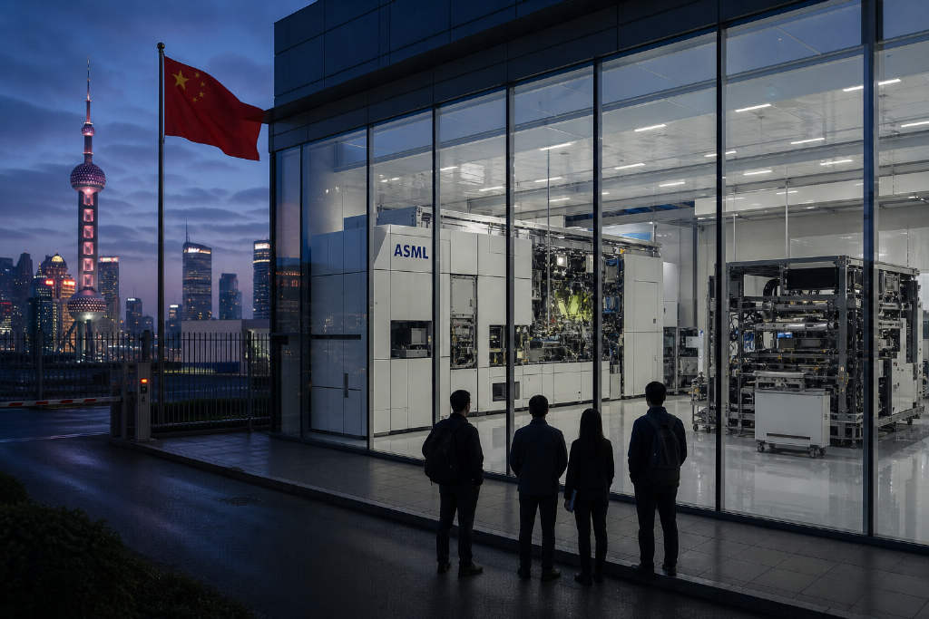
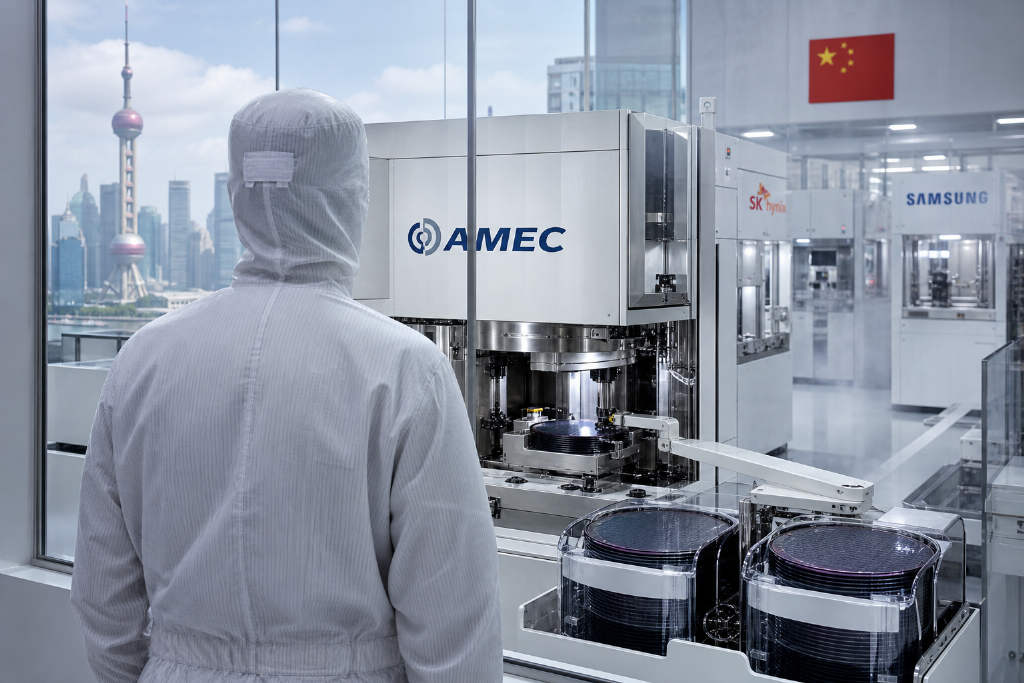
Elon Musk’s TeraFab chip manufacturing plan has moved from a compute-supply story into a lithography debate after speculation that the project may be aligned with a free-electron laser, or FEL, approach to extreme ultraviolet light sources. The discussion gained momentum after Musk posted 「FEL FTW」 on social media, a remark that many read as support for the idea. The core issue is whether FEL can attack one of the most entrenched positions in the semiconductor equipment business: ASML’s dominance in EUV lithography.
The article lays out why that question is drawing attention now. ASML’s laser-produced plasma, or LPP, light source enabled commercial EUV, but its limits are becoming more visible as the industry pushes toward 2 nm and below. Conversion efficiency remains low, tin debris contaminates costly mirrors, and power requirements keep rising. FEL backers argue their approach avoids plasma conversion, removes tin-droplet contamination, and could deliver much higher EUV output. xLight, which raised an oversubscribed $40 million Series B in July last year and later brought in former Intel CEO Pat Gelsinger as executive chairman, says its system could sharply raise fab productivity.
Even so, the broader field remains mixed. ASML is still expanding EUV and DUV output, advancing High-NA EUV, and posting rising sales and profit. At the same time, alternative paths including X-ray lithography, nanoimprint lithography, and electron-beam direct write are also developing, each with different trade-offs in cost, throughput, and manufacturability.