
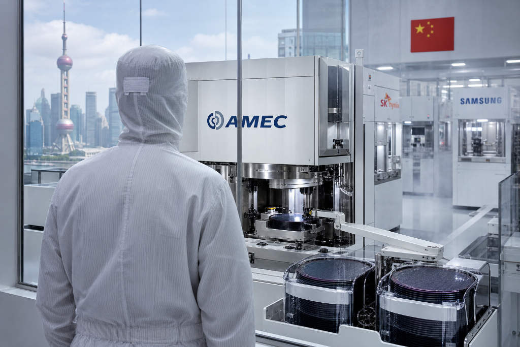
In early August, Reuters said Samsung Electronics and SK Hynix were looking at chipmaking gear from China’s Advanced Micro-Fabrication Equipment Inc. China, or AMEC, for possible use in their fabs in China. Reuters also said the two South Korean memory giants had quietly begun testing AMEC’s etching tools about two years earlier. Samsung later denied it, saying it had never weighed such a move. SK Hynix said nothing.
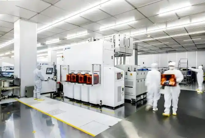
Even with that rebuttal, the article makes one thing plain: AMEC is already inside Taiwan Semiconductor Manufacturing Co.’s supply system, and Chinese firms are now shipping high-end semiconductor tools, including etchers, to top fabs around the world.
How AMEC started with etching tools
The story, the report says, goes back to March 2004 at SEMICON CHINA 2004 in Shanghai. There, Jiang Shangzhou met Yin Zhiyao. Jiang had already helped bring Richard Chang into what later became the SMIC story, and at the time he was deputy secretary-general of the Shanghai municipal government. Yin was then a senior vice president of research and development at Applied Materials and already a big name in global etching equipment. One more link between them: both had graduated from Beijing No. 4 High School.
Jiang, who studied radio engineering at Tsinghua University, had been trying to build Shanghai’s chip industry and had started turning his attention to semiconductor equipment, a layer even deeper than wafer fabs. The article says he asked Yin bluntly: "It seems etching machines are even more complicated than atomic bombs. Can we build one ourselves?"
Yin had spent 20 years in Silicon Valley, helped lead development of several generations of plasma etching tools, and held more than 60 patents, the report says. Going back to mainland China to launch a company in a field this hard made little financial sense then. Especially at his age and with his career standing. But three things changed his mind, according to the article: a family tradition of studying abroad and returning to China, Jiang’s pitch to build a homegrown etcher, and Richard Chang’s promise that SMIC could be the first customer.
In May 2004, Yin returned to Shanghai and founded AMEC. The piece says he did not bring back drawings or technical papers from the U.S. What the startup had was the know-how in the heads of Yin and his colleagues, RMB 50 million in seed money from the Shanghai government, and $1.5 million raised by the team.
That money disappeared fast. The article says Jiang introduced Yin to Chen Yuan, then governor of China Development Bank. Once Chen learned the team wanted to build etching tools, he backed it. AMEC then got a $50 million interest-free loan, giving its research and development effort real traction.
In June 2007, AMEC finished its first domestically developed high-end etching system. Then came trouble. Applied Materials sued Yin and several core employees in a U.S. court, accusing them of stealing trade secrets. The report says Yin put together a top legal team, spent two and a half years and $25 million on legal fees, and went through 6 million internal documents before clearing himself. In 2010, the two sides settled and agreed to share some patents.
The article says AMEC’s true advantage came from a strategy of developing two generations ahead. Back in 2004, when the company was founded, the world’s most advanced chip production lines were still at 90 nm. Yin still pointed the team toward 40 nm etching tools. The report quotes him this way: "Technology in the integrated circuit industry moves too fast. Only by developing two generations ahead can you hold the initiative when the market actually needs the equipment."
And the article says that bet paid off more than once. In 2015, AMEC’s plasma etchers reached quality and throughput levels comparable to U.S. tools. After that, the U.S. Commerce Department removed a long-running export embargo on that equipment category to China. By the end of 2018, AMEC’s self-developed 5 nm etcher had passed validation at TSMC and was used on the world’s first 5 nm production line. The piece also says AMEC became the only mainland supplier to get into TSMC’s 7 nm etching equipment supply chain.
Behind that progress stood an international team from more than a dozen countries and regions, with several thousand employees across more than 30 disciplines. To show just how exact these machines are, Yin used a metaphor the article repeats: "If you carve characters onto a grain of rice, 200 characters is generally the limit. Our etching machine is like being able to carve 1 billion characters onto that same grain of rice."
The broader map of China’s equipment makers
The report then jumps to a roundtable in August 2024, around the fifth anniversary of the STAR Market. Four executives were there: AMEC chairman Yin Zhiyao, Piotech chairman Lü Guangquan, Hwatsing general manager Zhang Guoming, and Skyverse chairman Chen Lu. The talk centered on the road toward self-controlled semiconductor equipment in China.
Lü, like Yin and Chen, came back from overseas after years in the business. He earned a semiconductor doctorate in San Diego, California, spent 20 years in process technology research and development at companies including Novellus in the U.S. and Aixtron in Germany, and joined Piotech’s predecessor in 2014. He picked PECVD thin-film deposition equipment, then still a largely empty space in China, as the company’s focus. The article says Piotech became the only domestic company to industrialize PECVD and SACVD applications for integrated circuits.
Chen Lu, a classmate of Yin at the University of Science and Technology of China, entered USTC’s special class for gifted youths at age 15, later earned a doctorate in optical physics from Brown University, and worked as a senior scientist at KLA-Tencor and Rudolph Technologies in the U.S. He returned to China in 2010 to join the Institute of Microelectronics at the Chinese Academy of Sciences, and formally founded Skyverse at the end of 2014. The company began in rented residential space. Later, it became a STAR Market-listed leader in China’s wafer inspection equipment segment.
Hwatsing is framed differently. Homegrown. The article says Lu Xinchun, still a professor in Tsinghua University’s Department of Mechanical Engineering, industrialized chemical mechanical polishing technology with his team in 2013 and incubated Hwatsing. A year later, the company turned out its first 12-inch CMP system, breaking an international monopoly. Hwatsing listed on the STAR Market in 2022. Its CMP equipment for process nodes above 14 nm now shows no technology gap with global leaders, the report says, and its products have entered production lines at SMIC, Yangtze Memory Technologies, ChangXin Memory Technologies and Intel.
The piece says these four companies, none of them much older than two decades, have each become heavyweights in their own corner. And they are far from the only ones. A wider group of companies has been filling in the full map of China’s semiconductor equipment industry.
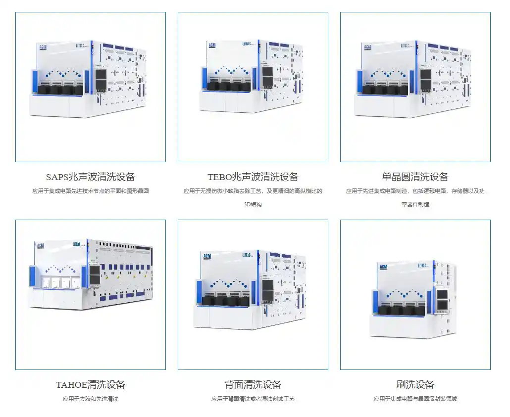
In chip cleaning equipment, the report points to ACM Research Shanghai founder Wang Hui, whose path it says looked a lot like Yin’s. Wang founded ACM Research in Silicon Valley in 1998 and developed stress-free copper polishing technology, but the market saw it as too early and the company at one point came under pressure to sell. Jiang Shangzhou urged Wang not to sell and to move the company to Shanghai instead. Wang took the advice and set up ACM Shanghai in 2005. The article says the company’s products had already entered global fabs including Hynix more than 10 years ago, and that its SAPS/TEBO megasonic cleaning technology and Tahoe single-wafer chamber cleaning technology solved major industry cleaning problems.
NAURA is presented as a different sort of domestic success story. A platform company. Reorganized in 2017, NAURA traces its roots to the state-owned 700 Factory in Jiuxianqiao, Beijing, founded in 1965. The article says it drew support from Beijing state-owned capital, as well as Peking University, Tsinghua University and the Chinese Academy of Sciences, and also got backing from the National Integrated Circuit Industry Investment Fund. Its path leaned on acquisitions: in 2018 it bought assets and technology from U.S. cleaning equipment maker Akrion, and in 2020 it acquired radio-frequency power company Beiguang Technology, gradually building up a portfolio spanning etching, PVD, LPCVD, cleaning tools and oxidation furnaces.
The report says NAURA is now China’s broadest semiconductor equipment platform company by product coverage, and the strongest domestic leader in the field, with revenue of RMB 39.353 billion in 2025.
Other names come up too. Kingsemi is credited with closing a domestic gap in coating and developing equipment. Leadmicro is described as a local leader in ALD, or atomic layer deposition. Shanghai Micro Electronics Equipment Group also appears, though public information on it is much thinner and it operates in the hardest lithography segment. By around 2020, the article says, China’s semiconductor equipment map had been pieced together by companies entering through different niches but sharing the same determination to keep pushing at choke-point technologies.
Domestic fabs and equipment makers grew together
According to the article, all four executives at the 2024 discussion landed on the same point when they talked about the strengths and weaknesses of China’s semiconductor equipment industry: domestic equipment makers and domestic fabs have been strengthening each other.
They said Chinese equipment companies still lag global leaders by a wide margin. But they are also building their own advantages, including differentiated innovation, joint problem-solving with local fabs, and custom development.
SMIC is named as one of the biggest backers. In 2017, when it hired Liang Mong-song away from TSMC, its 28 nm yield was still under 60%, progress at advanced nodes had stalled, and it had just come through a patent dispute. The article says Liang needed only 298 days to push 14 nm FinFET yield above 90%. Later, he led a team that used existing DUV lithography tools and multiple patterning to make the N+1 process, with performance close to 7 nm, sidestepping U.S. export restrictions on EUV lithography systems.
The report says that same refusal to accept technical dead ends also showed up in SMIC’s attitude toward domestic tools. Core products from more than a dozen Chinese equipment and materials companies, including Piotech, Kingsemi, NAURA, AMEC, Shanghai Sinyang and National Silicon Industry Group, first passed validation on SMIC production lines before finding a broader market and entering a cycle of technical and commercial growth.
The rules in semiconductor equipment are brutal. A new tool trying to replace an incumbent has to prove performance and cost efficiency, then survive a fab validation cycle that can take years. Miss at any point and years of work can vanish. The article says SMIC, almost by itself, used its lines to incubate the first batch of domestic semiconductor equipment challengers. That deployment-led development model is still there.
Last September, the report says, SMIC was reported to be testing a domestic DUV lithography machine developed by Shanghai startup Yuliangsheng. The article calls that test a key step in China’s push to break through what it describes as lithography’s final fortress.
Export controls kept tightening
The article links the tighter relationship between domestic fabs and domestic equipment suppliers to rising U.S. export controls. Those restrictions pushed Chinese fabs toward heavier reliance on domestic tools. They also moved semiconductor equipment higher on the strategic agenda and pulled in more state and social resources.
At SEMICON China 2023, Yangtze Memory Technologies chairman Chen Nanxiang made a sharp remark quoted in the report: "The equipment was purchased legally and in compliance with regulations. If there were fairness, and the equipment is left paralyzed on the factory floor because the equipment maker refuses to sell parts when it breaks down, then the equipment maker should buy it back with cash." The article says he was speaking in the context of U.S. export controls that had left Chinese fabs unable to buy spare parts even for lithography machines that had already been installed for years.
- In May 2019, Huawei was placed on the Entity List.
- In December 2020, SMIC was restricted from purchasing advanced process equipment for 10 nm and below.
- In October 2022, the U.S. Commerce Department expanded controls to cover almost the entire semiconductor equipment chain needed for logic chips below 14 nm, DRAM below 18 nm and NAND above 128 layers.
- In October 2023, the control list was expanded again.
- In December 2024, another 24 Chinese semiconductor equipment and tool companies were added to the Entity List, extending controls across etching, deposition, lithography, ion implantation, metrology and cleaning equipment.
Each round, the article says, bit deeper into Chinese fabs’ access to advanced foreign equipment and even after-sales maintenance for spare parts. But the restrictions did not choke off China’s semiconductor industry. In the report’s telling, they forced domestic fabs and equipment companies into closer coordination and pulled more capital and resources into the whole chain.
Funding, localization rates and recent industry figures
The article says the National Integrated Circuit Industry Investment Fund has completed three phases since 2014, with total committed capital above RMB 680 billion. The third phase, set up in 2024, had registered capital of RMB 344 billion, a global record for a dedicated semiconductor fund. According to the report, nearly half of that money went to equipment and materials.
Citing data from the China Electronic Special Equipment Industry Association, the article says China’s overall localization rate for semiconductor equipment rose from less than 5% to about 20% by 2025. In etching, thin films, cleaning and polishing, Chinese companies now have the technical ability and corporate strength to compete directly with global leaders.
At the same time, the article says, 20% still means huge gaps remain. Advanced lithography is still one of the hardest. In March 2026, NAURA chairman Zhao Jinrong and other semiconductor industry figures jointly published a paper calling for a nationwide effort to build a Chinese lithography champion.
On operating performance, the report cites National Bureau of Statistics data showing profit in China’s integrated circuit industry rose 18.5 times in the first seven months of this year. It says Yangtze Memory and ChangXin Memory recorded a combined loss of RMB 35.5 billion in 2023, then combined profit of RMB 58.1 billion in the first quarter of 2026. Cambricon lost RMB 848 million in 2023, then posted profit of RMB 2.311 billion in the first half of 2026. SMIC earned RMB 4.823 billion in 2023 and RMB 4.467 billion in the first half of this year.
With chip companies posting sharply better numbers, equipment makers such as AMEC and NAURA have also hit the best performance in their history, the article says.
On Aug. 28, Li Chao, deputy director-general of the Policy Research Office and spokesperson for the National Development and Reform Commission, said at the commission’s August press conference that China has a super-large market, a complete industrial system and rich talent resources, giving the integrated circuit industry a solid foundation, wide room for growth and strong momentum. He said the industry is speeding into a globally competitive emerging pillar sector.
Li also said that from January to July this year, capacity utilization at China’s major wafer foundries stayed above 90%, while integrated circuit exports reached RMB 1.49 trillion, up 91.6% year on year. He added that the next step would be to stay focused on the goals set in the 15th Five-Year Plan outline, use the strengths of China’s new nationwide system, and push for decisive breakthroughs in key integrated circuit technologies across the full industrial chain.
The original article ends by saying bigger good news may not be far off for China’s chip equipment sector. It was attributed to the WeChat account HSTL8888, with authorship also listed as HSTL8888.