

Elon Musk’s TeraFab chip plan has opened a new line of discussion around lithography after market chatter suggested the project may be tied to a free-electron laser, or FEL, light-source route rather than the conventional EUV path dominated by ASML.

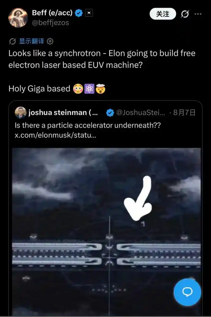
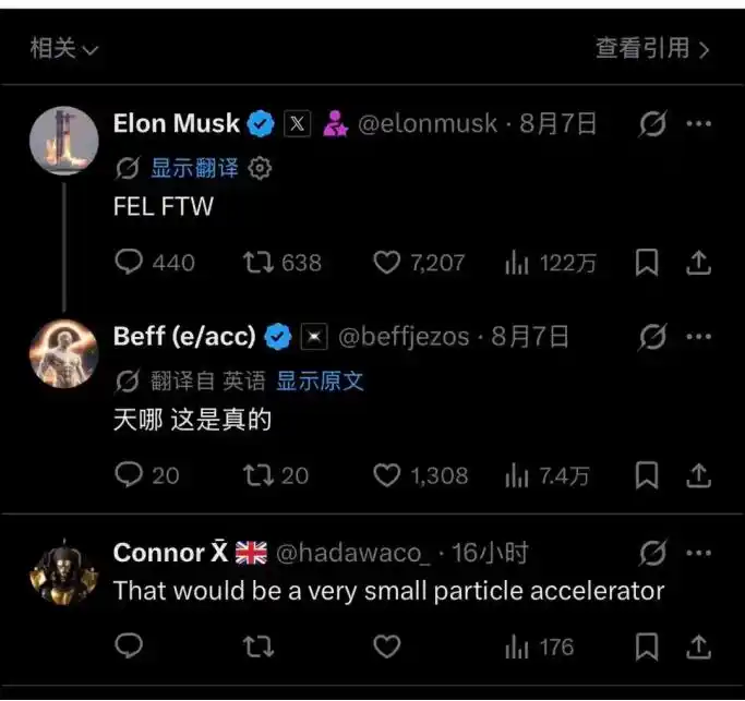
Musk first unveiled TeraFab in the spring of 2026. His stated rationale was simple: SpaceX and Tesla will need at least 1 terawatt of compute in the future, a scale he said is more than 10 times current global chip supply capacity. This month, the focus shifted from chip manufacturing capacity to lithography equipment after a blogger said TeraFab’s disclosures pointed to an FEL direction. Musk then posted 「FEL FTW」 on social media, a line that was widely read as indirect support for that interpretation. Combined with TeraFab’s long, narrow factory design, the FEL route has become the most discussed possibility.
Under earlier plans, TeraFab is meant to build an integrated chip manufacturing base that would produce both logic and memory chips while combining lithography, packaging, and testing inside a single facility.
TeraFab and the renewed focus on FEL
The idea did not emerge in isolation. In July last year, semiconductor startup xLight said it had closed an oversubscribed $40 million Series B round. The company said the capital would be used to push FEL research with the aim of breaking through the physical limits of current EUV lithography and supporting volume production of 2 nm and more advanced chips with a new light source. In March last year, former Intel CEO Pat Gelsinger wrote on LinkedIn that he had joined xLight as executive chairman.
That sequence brought FEL back into a serious industry conversation. Instead of competing head-on with ASML on complete lithography systems, the argument around TeraFab and xLight centers on the light source itself.
Why the industry is revisiting EUV light sources
In the AI chip supply chain, ASML remains the only company in the world currently able to build EUV equipment. The article says it holds more than 90% of the lithography equipment market.
ASML’s EUV tools use a laser-produced plasma, or LPP, EUV source. A 30 kW carbon dioxide laser strikes tin droplets ejected from a nozzle at a rate of 50,000 drops per second. Each droplet is hit twice, which means 100,000 laser pulses every second. The impacts turn the tin into plasma, and transitions between high-charge tin ion energy levels produce EUV light at a wavelength of 13.5 nm.

LPP made commercial EUV possible, but its physical limits are becoming more pronounced as process nodes continue to shrink.
The first issue is conversion efficiency. The 13.5 nm wavelength is much shorter than the 193 nm light used in mainstream DUV tools, which is why EUV can define smaller features on silicon. ASML mainly relies on carbon dioxide lasers from Cymer in the US to generate tin plasma. The conversion efficiency from drive laser to tin plasma is 5.5%, according to the article. The carbon dioxide laser itself has an electro-optical efficiency of about 10%, and once transmission losses in the collector mirrors are included, actual EUV utilization from the power grid to the wafer is generally below 0.5%.
The second issue is tin debris contamination. During plasma generation, high-speed sputtered tin ions and neutral debris deposit on the surface of extremely expensive multilayer collector mirrors, cutting reflectivity and reducing service life.
The third issue is source power. Current LPP-EUV sources have reached about 600 W of maximum EUV output. Yet manufacturing at the 2 nm node and below requires more than 1.5 kW of EUV power. At today’s 500 W to 600 W level, EUV often depends on multiple exposures to build enough photon dose and offset the source-power shortfall.
ASML said in February that by 2030 it plans to introduce a new source system with as much as 1000 W of power, raising the productivity of next-generation high-NA EUV tools by 50%. By 2030, wafer throughput per EUV tool is expected to rise from 220 wafers per hour to 330 wafers per hour.
How FEL differs from LPP
FEL does not rely on plasma conversion. In an FEL system, an electron gun emits an initial beam, and a linear accelerator, with advanced designs often using a superconducting linear accelerator, pushes that beam close to the speed of light. The high-density relativistic electron beam then enters an undulator formed by a periodic alternating magnetic field. The electrons oscillate laterally and emit spontaneous radiation. The radiation field continuously modulates the beam, causing the electrons to form microbunches with spacing set by the radiation wavelength. Those microbunched electrons emit coherent radiation, a positive feedback loop forms, and the radiation intensity grows exponentially. With techniques such as seed injection, the system can ultimately produce a wavelength-stable EUV beam.
That is why FEL-generated extreme ultraviolet light is being discussed as a candidate for next-generation lithography. The relevant band is shorter than today’s 13.5 nm EUV and closer to soft X-rays. Based on public information cited in the article, xLight is targeting precise tunability in the 2 nm to 7 nm Blue-X band, also described as the 「beyond EUV」 band.
Supporters point to two main advantages. There is no process involving tin droplets being struck and no plasma sputtering inside the optical path, so the vacuum chamber does not suffer from metal debris deposition. The article also says an EUV-FEL source can generate more than 10 kW of EUV power, enough in principle to supply more than 1000 W of EUV power to 10 EUV lithography tools at once without causing tin contamination on Mo/Si reflective mirrors.
Three paths are now visible in lithography
The article breaks the field into three broad tracks: incremental EUV improvement, a light-source reset within EUV, and non-EUV alternatives. All three are active, though EUV iteration remains the main line.
1. ASML’s incremental EUV advance still leads
ASML remains firmly in command of the mainstream market. Net sales in the first quarter reached 8.8 billion euros, with net profit of 2.8 billion euros. In the second quarter, total net sales were 9.326 billion euros and net profit came to 2.918 billion euros. The company also raised its full-year outlook sharply for the second time this year, lifting expected 2026 sales to 43 billion euros to 45 billion euros.
The jump reflects a wider buildout in technology infrastructure. Amazon, Google, and Microsoft are spending hundreds of billions of dollars on infrastructure, which has driven demand for advanced AI chips. Fabs producing both logic and memory are expanding, and demand for lithography tools has tightened accordingly.
Capacity plans are also aggressive. Based on a 2026 plan for about 65 low-NA EUV systems, ASML aims to expand capacity by 30% in 2027 and is studying another 30% increase in 2028. For immersion DUV, it plans 2026 capacity of about 130 systems, followed by a 30% increase in 2027 and is studying another 30% rise in 2028.
ASML’s next flagship is High-NA EUV. The system uses a numerical aperture of 0.55, can reach 8 nm resolution, supports 3 nm and below, and creates a technical base for the 1 nm node. The article says a single exposure on High-NA EUV improves patterning fineness by 1.7 times, lifts imaging contrast by 40%, and enables transistor density 2.9 times that of the previous generation, reducing chip power consumption and increasing computing speed.
Still, High-NA EUV adoption has been slower than hoped. A single machine costs about $400 million, nearly twice the price of a conventional EUV system, and line integration is difficult. Chang Hsiao-Chiang, TSMC’s senior vice president for business development and global business and co-COO, said ahead of the company’s annual technology forum that TSMC currently has no plan to deploy the ASML High-NA EUV tools designed for next-generation processors.
2. Light-source innovation targets the core of the system
This is the lane where TeraFab and xLight are being placed. The strategy is not to displace ASML’s optical system leadership directly, but to break through at the source. If the light source can be swapped independently, chipmakers would not need to replace large sections of supporting lithography, etch, deposition, and inspection equipment. Replacing the source alone could improve output and cost structure, which is why the article describes it as an attractive plug-and-play upgrade path for fabs.
xLight says its FEL system delivers more than four times the power of existing systems. It also says deploying xLight FEL at existing US fabs could lift production efficiency by 50% while removing the need for consumables such as tin or hydrogen. In newly built fabs, xLight says production efficiency could increase by 100%. The company frames that as a way for manufacturers to produce smaller-feature, more efficient chips and extend next-generation lithography.
If the light source can truly be replaced as an independent module, ASML’s pricing power could weaken structurally. But the article also notes that ASML examined the FEL EUV route about a decade ago and ultimately judged the risk too high, choosing LPP EUV instead. That leaves the central question unresolved: whether FEL can be brought into volume manufacturing, and when.
Other source routes are also under development. San Francisco startup Substrate, founded in 2022, has chosen a particle-accelerator-based X-ray lithography path. China is also pushing domestic EUV source technology. According to public information cited in the article, multiple teams in China are exploring different routes, including reverse engineering around existing LPP technology, with a goal of breakthroughs between 2028 and 2030. Among them, Harbin Institute of Technology and other institutions are trying to develop a laser-induced discharge plasma, or LDP, lithography scheme. In that design, tin is vaporized between electrodes and a high-voltage discharge excites the plasma. The structure is simpler than LPP and requires less floor space, though its power density remains limited and whether it can support mass production is still unclear.
3. Non-EUV alternatives keep moving
The third group consists of routes that bypass EUV altogether.
Nanoimprint lithography, or NIL, is one of the fastest-moving commercial options. It presses patterns directly with a physical template and does not require a complex optical system or source, which means lower equipment cost and lower power consumption than EUV. Canon in Japan has already pushed NIL into volume production for memory chips. Its resolution still does not match High-NA EUV, but in memory applications where line-width demands are relatively looser, NIL has shown cost competitiveness.
Electron-beam direct write, or EBL, follows a very different path. In essence, electron-beam lithography is a direct-write process that uses a focused electron beam to expose resist point by point, with electromagnetic control used to define patterns precisely. It does not rely on masks, which makes it especially useful in research stages where designs change frequently, including quantum devices, novel material structures, prototype chips, and mask making.
So far, though, electron-beam lithography has largely remained in research and limited-scale use. The bottleneck is not resolution but throughput. Electron-beam direct write is a serial exposure process. Point precision can be high, but overall throughput is too constrained for wafer-scale volume manufacturing. In research settings, that same slowness buys flexibility. For teams repeatedly changing layouts, testing physical models, or exploring new device structures, skipping mask production often matters more than higher exposure speed.
The article’s closing point is that EUV now looks like a long-running incumbent. Its technical bottlenecks are real, but so is the ecosystem ASML has built around it over two decades. A new entrant does not change the market by running faster alone. It has to persuade the whole track to accept a new set of rules.
By that framing, Musk’s TeraFab is a high-stakes bet: a bet that FEL can move from the lab to the fab, that a plug-and-play source replacement can get around ASML’s patent barriers, and that demand for 1 terawatt of compute is enough to support an entirely new supply chain. What comes next for next-generation lithography may not take long to become clearer. But once Musk posted 「FEL FTW」, the business was no longer being discussed as ASML’s game alone.
The original article was published by the WeChat public account 「半导体产业纵横」 (ID: ICViews) and written by Feng Ning.