
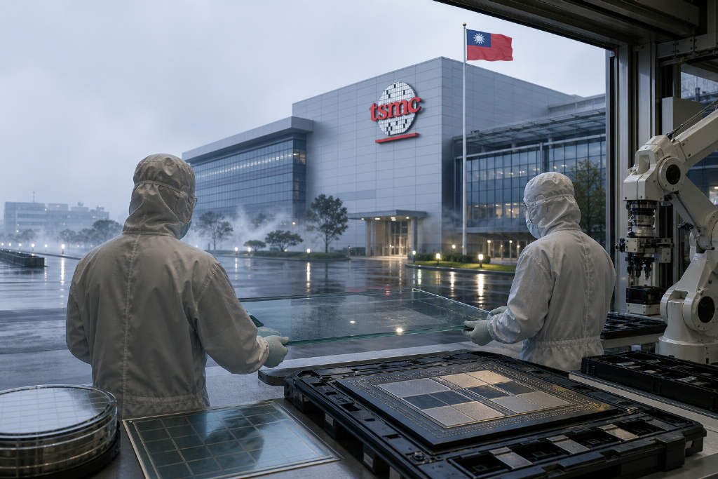
Demand for heterogeneous integration in AI chips is climbing across compute, memory, and communication bandwidth, and package sizes have expanded from "2x reticle" to "4 to 5.5x reticle" in the past two years. That rapid increase in package size has intensified concerns over warpage, turning glass substrates into one of the semiconductor sector's most discussed material themes.

ABMedia, citing Statementdog's industry report titled Glass Substrate Industry Outlook and Competitive Landscape, said the real scaling window for the theme is likely to fall between 2027 and 2029. Suppliers across the upstream, midstream, and downstream parts of the chain have already started positioning for that timeline.
Two different roles: carrier and substrate
Glass substrates are often discussed together with panel-level packaging, or PLP, but the two are not inherently tied to each other. The report first distinguishes the role glass plays inside semiconductor packaging, where it serves two very different purposes.
The first is as a temporary carrier. Chips and packaging materials are fixed onto a glass carrier during processing, and the carrier is removed after manufacturing is completed and the chip is delivered to the customer. In that form, the glass does not remain in the final product. The report said this use case is already widely seen in wafer-level packaging, CoWoS, and SoIC.
The second is as a substrate or an interposer. In that case, the glass remains inside the package after the process is finished and becomes part of the final product. That is the use drawing most of the recent market excitement and industry discussion.
Structurally, a substrate sits between the bare die and the printed circuit board, or PCB. Signals move from the chip's internal metal layers to the substrate wiring and then to the PCB. An interposer adds an extra, denser connection layer, so the signal path runs through the chip, the interposer, the substrate, and then the PCB.
In a broad sense, the term "glass substrate" covers both glass substrates and glass interposers, but their commercialization timelines differ by a wide margin. The report said glass substrates are closer to volume production, while glass interposers remain at a much earlier stage despite concept work and prototypes.
Substrates and interposers are needed because chip and PCB line dimensions are vastly different. Advanced-process chips have already moved into nanometer-scale line width and spacing, while PCB routing is still measured in micrometers. The gap is more than a thousandfold, making direct signal connection impractical. Substrates and interposers act as transition structures that gradually scale the routing dimensions.
NVIDIA has proposed a CoWoP concept that attempts to remove the substrate and connect the chip or interposer structure directly to the PCB. The report said that, in theory, this could shorten the signal path and reduce transmission loss. For now, though, the technology remains difficult to realize, and substrates still serve as an essential bridge between chips and PCBs.
Why glass is being considered
The report said glass is being viewed as a candidate material for next-generation substrates because it combines three strengths that conventional organic materials have struggled to balance at the same time.
- Its coefficient of thermal expansion, or CTE, can be adjusted depending on the materials paired with it
- It has high rigidity and resists bending deformation
- It offers a very flat surface
Those properties can help reduce warpage risk during repeated heating and cooling in large packages. They also support finer wiring and higher layer counts, both of which are increasingly important as AI-driven heterogeneous integration pushes package areas larger.
The tradeoff is that high rigidity comes with fragility. Harder material usually means less flexibility and a greater risk of cracking. The report identified three major bottlenecks for mass production at this stage.
- Through-glass vias, or TGVs, carry a risk of brittle damage along the via wall
- Copper wiring does not adhere strongly enough to the glass surface
- The transparency of glass makes it hard to reuse conventional optical inspection equipment, so new inspection solutions are needed
If both sides of the glass are to carry wiring, holes must be drilled to connect upper and lower circuits. The report described that TGV step as the core technical challenge and a major reason why existing packaging processes need a new process window when glass is introduced.
Commercialization timeline: 2027 trial production, 2028-2029 scale-up watch
Statementdog estimates that commercialization will move in stages. Limited commercial use could appear as early as 2027, with optical communications seen as a possible first application. Large-scale production, however, is expected to wait until 2028 to 2029.
Company timelines are not aligned. Samsung Electro-Mechanics and Absolics are moving relatively aggressively, targeting 2027. Ibiden and DNP are taking a more cautious stance, with schedules extending into 2028 to 2030.
The report said the decisive marker for real volume adoption will be whether TSMC brings glass substrates into its CoWoS advanced packaging lines. It places that observation point around late 2028 to early 2029, and identifies it as the industry's most important signal.
Glass interposers are expected to trail behind glass substrates because they are harder to manufacture and require tighter integration with chips. Most estimates in the report place their maturation after 2030.
Supply chain map: materials, panel processing, and back-end packaging
The report divides the glass substrate supply chain into three broad segments: upstream glass base materials, midstream panel-level processing, and downstream TGV via processing plus multilayer packaging.
Upstream glass base material suppliers
- Corning (GLW)
- AGC
- Nippon Electric Glass (NEG)
- Schott
Midstream panel supply chain companies
- DNP
- TOPPAN
- JNTC
- Innolux (3481)
- BOE
- Vogo Optoelectronics
Glass substrate and back-end stacking companies
- SEMCO Samsung Electro-Mechanics
- Absolics
- Ibiden
- Shinko Electric
- Unimicron (3037)
- Nan Ya Printed Circuit (8046)
Wafer manufacturers
- Intel (INTC)
- TSMC (2330)
According to the report, the most intense competition right now is centered on TGV drilling and metallization, where many companies are trying to secure a position around the main bottleneck. Over the longer term, the report argues that stronger moats may emerge at both ends of the chain: upstream glass base materials and downstream high-end multilayer stacking integration. In the high-end market, it said leadership could still tilt toward established substrate makers and TSMC.
For the semiconductor industry and investors tracking the supply chain, glass substrates are not only a materials story. The report frames them as part of the next reshuffle in advanced packaging competition.