
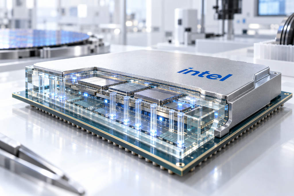
Intel has obtained a U.S. patent that describes embedding MicroLEDs inside a CPU package. According to Tom’s Hardware, the patent application was filed in 2022. The design uses a glass substrate and through-glass vias, or TGVs, so MicroLEDs can connect directly to a die and receive power. The concept could be used to light up text on a processor package and show chip operating status. It also sits close to broader trends in glass substrates and co-packaged optics, or CPO.

How the patented package is structured
The report says the patent is titled “IC Package with Micro LEDs.” In the proposed structure, a glass substrate sits in the middle, with one package substrate attached above and another below. Part of the semiconductor die is embedded into the glass substrate, leaving the back side exposed, though the patent also says the die could be fully embedded.
MicroLEDs would connect to the die either directly or through nanowires. Power and signals would be delivered to the die through TGVs running across the glass substrate. The patent says the MicroLEDs can emit red, green, and blue light.
On the process side, the filing describes using laser treatment and etching to create holes and die cavities, then forming TGVs through copper electroplating. A die carrying the MicroLEDs is then embedded, and a silicon nitride layer bonds the glass to polymer package substrates on both sides.
More than lighting effects
The patent describes several possible uses. A processor could drive the MicroLEDs to indicate that a specific function is running, or the LEDs could be used purely for appearance. The filing also says a real product could place MicroLED arrays on one or more IC packages, which means multiple lighting functions could be integrated in theory.
For diagnostics, the MicroLEDs could use fixed light patterns to show whether testing has completed or failed, reducing the need for external indicator lights on a motherboard or peripheral hardware. Tom’s Hardware also notes that the patent does not describe a complex diagnostic system. Separate analysis cited in the report suggests the architecture could become part of in-situ optoelectronic testing during packaging.
Thermals remain a constraint for any appearance-focused use. High-power chips need heatsinks, and those heatsinks could block LEDs placed on the package surface. The report’s author says that could limit the design to lower-power chips or require heatsink designs that leave part of the package exposed.
Part of Intel’s longer push into glass substrates
The patent builds on Intel’s longer-term work in glass substrate technology. Tom’s Hardware says Intel has been developing glass substrates since the early 2010s. In January this year, Intel showed an engineering sample of a glass-core package combined with EMIB multi-die packaging at NEPCON Japan. In May, at ECTC, the company presented a 24-layer glass core panel with copper-filled TGVs and two embedded EMIB bridges, and shared progress toward mass-production validation.
Compared with conventional organic substrates, glass substrates are seen as offering higher flatness, better heat resistance, a lower coefficient of thermal expansion, and lower signal loss. That is why they are widely viewed as a key material for next-generation high-performance packaging.
Why attention is shifting to CPO
The bigger point of interest is not the lighting effect itself, but what the patent might imply for CPO. Demand for AI compute is pushing up data traffic between GPUs and accelerators, while conventional electrical interfaces are running into bandwidth and power limits. That has increased interest in packaging architectures that integrate optical components.
AUO has already been active in that direction. Chain News reported last week that the industry has been discussing possible cooperation between Intel and AUO. AUO Chairman Paul Peng had also said during an earnings call that the company had established a position in advanced packaging and glass substrates and was developing products with partners, though he did not identify them because of confidentiality agreements.
Tom’s Hardware also said AUO showed Micro LED optical communication equipment for AI data centers at SEMICON Taiwan 2026, using a MicroLED transmitter paired with a photodetector receiver. Intel had previously shown a co-packaged optical I/O chip as well. If the two companies do work together, the report says that could speed up Intel’s progress in optical interconnects inside packages.
A patent is not a product
The report draws a clear line here. The patent does not propose an optical interconnect application, and it does not claim high-speed optical communications. What it describes is a packaging technology that could support such systems. A complete optical interconnect module would still need a receiver side and fiber-based solutions.
The application is also more than four years old. Whether Intel will actually bring MicroLEDs into a commercial processor package remains unknown.