
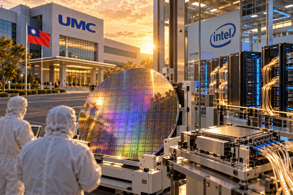
Intel is making a bigger bet on silicon photonics as it looks to open a new front in optical interconnects for AI data centers. Citing Economic Daily News, the source article said United Microelectronics Corp. (UMC) has formed an alliance with Intel and obtained a 12-inch silicon photonics technology license from Belgium-based imec, as it builds out work on silicon photonics chips and co-packaged optics (CPO).
Intel says it can mass-produce InP on 12-inch wafers
Intel said it has the manufacturing capability to integrate indium phosphide (InP) on 12-inch wafers at mass-production scale, and described that capability as the only one of its kind globally. InP is a key material for laser light sources, and stable production on larger wafers is central to the cost profile and scaling speed of silicon photonics.
The company wants to use that capability in optical interconnects for AI data centers, replacing part of copper-based transmission with optical signals to handle rising data traffic between GPUs and AI accelerators. The source article noted that the "only one globally" claim is Intel’s own description and has not been independently verified by a third party.
OCP 2026 roadmap points to deployment within two years
At the OCP 2026 Summit, Intel laid out its silicon photonics roadmap. Nic Dubé, vice president of Data Center Systems and Solutions, described silicon photonics as a "golden hammer" and said the industry has discussed it for years as a standard approach, while Intel’s team is aiming to get the technology deployed in real-world settings within the next two years.
Dubé said conventional copper links are nearing physical limits in three areas: transmission distance, bandwidth density at the package edge, and energy consumed per bit. Intel’s position is that silicon photonics can address all three at the same time.
On platform design, Intel said it is using a highly stable light source while also supporting industry-standard external light sources, leaving room for different architectural choices. It also said it will provide multi-wavelength light sources supplied by U.S. wafer fabs.
UMC secures imec license and advances 12 nm work with Intel
The report said UMC is one of the Taiwanese chipmakers with the clearest positioning in this area. In addition to obtaining imec’s 12-inch silicon photonics technology license, UMC already has a process collaboration base with Intel. The two companies are jointly developing a 12 nm FinFET process that combines UMC’s foundry experience with Intel’s transistor technology, with production planned at the Ocotillo campus in Arizona to broaden manufacturing options for customers.
That 12 nm program is expected to provide customers with process design kits (PDKs) and related IP starting in 2026. Tape-outs are scheduled for 2027, followed by commercial mass production at the end of 2027. The target applications include Internet of Things chips, Wi-Fi, and high-speed interface chips.
Intel’s CPO effort also reaches the packaging side
Intel’s CPO work is not limited to the wafer manufacturing side. The source article said industry chatter last month pointed to talks between Intel and AUO covering advanced packaging technologies including glass substrates, through-glass vias (TGV), and Micro LED, with the same focus on CPO and integration for high-density computing chips.
From wafer processes and packaging to light sources, Intel is assembling a broader optical interconnect stack, and the article said multiple Taiwanese suppliers may have opportunities to enter the supply chain at different points. Even so, neither side has disclosed customers, orders, or revenue contribution tied to silicon photonics, and Intel’s two-year deployment target still remains to be tested by actual rollout progress.