


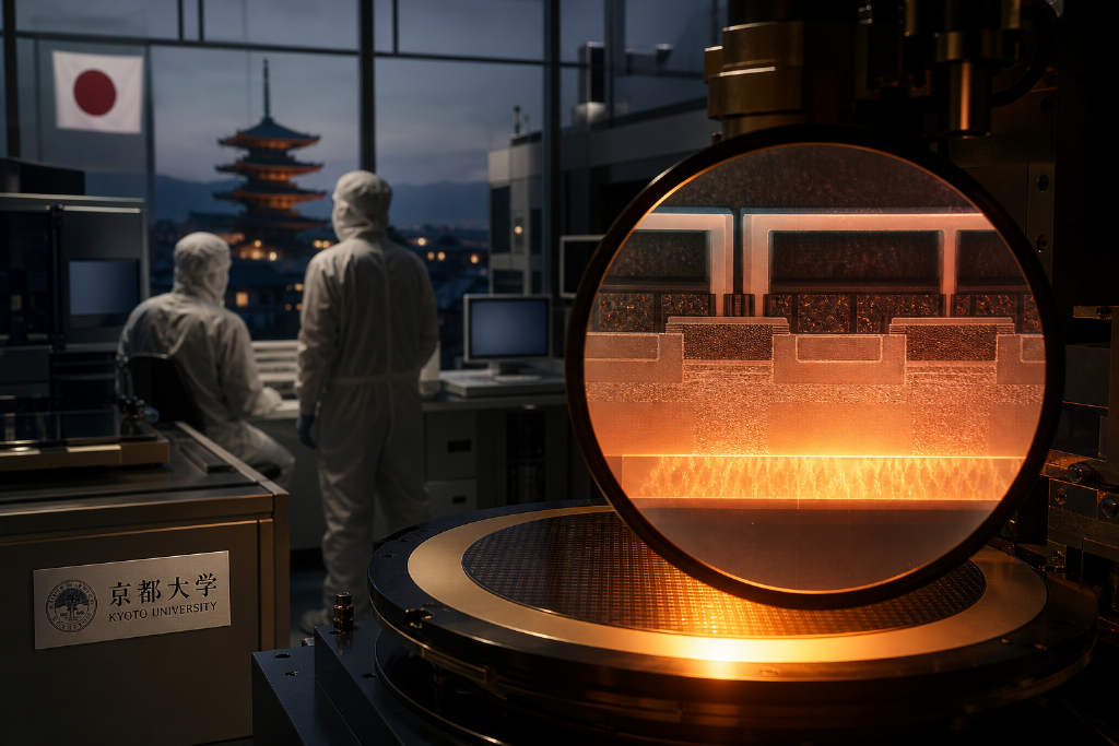
Kyoto University has developed a silicon carbide (SiC) transistor that can withstand temperatures of 600°C, far beyond the range where conventional silicon chips stop working at around 250°C and above. The project uses a bottom-gate design and a double-well isolation structure to deal with voltage drift and current leakage at extreme temperatures, while staying compatible with existing commercial wafer-fab manufacturing processes.
Ion implantation was a central process challenge
Ion implantation is the standard doping step used in commercial semiconductor fabs. It introduces selected impurities into a semiconductor to change its electrical behavior. Because it is already part of mainstream wafer manufacturing, using the same process for a new SiC transistor design would make it easier to fit into existing production equipment and improve the chances of scaling output.
The difficulty comes from the channeling effect that appears during ion implantation. That effect can drive dopants deeper than intended. In a conventional top-gate design, the source article says, this leads to severe threshold-voltage drift of more than 2V. Kyoto University’s bottom-gate structure was designed to counter that problem.
How the bottom-gate and double-well design works
According to Kyoto University’s research as described in the report, the team combined a bottom-gate layout with a double-well structure to tackle high-temperature voltage drift and leakage separately.
For voltage stability, the gate electrode is placed beneath the channel. That arrangement captures and compensates for dopants that scatter deeper than expected during ion implantation. The report says the difference between the design target and the measured threshold voltage was reduced to within 0.1V at 400°C.
For leakage control, the team focused on what happens when the semi-insulating SiC substrate below the transistor loses its insulating behavior at very high temperatures. In that situation, leakage current can pass through the entire wafer. To block that path, the researchers introduced a double-well structure that isolates each device inside its own pn junction, removing the need to rely on the substrate for insulation. The article says this brought residual leakage at high temperature down to a level close to the theoretical lower limit of the SiC material itself.
Stable operation at 600°C
Those two structural changes allowed the SiC transistor to maintain stable operation at 600°C. That is the central technical result highlighted in the report. Conventional silicon chips generally stop functioning at around 250°C, so the gap between the two temperature ranges is substantial.
Target applications are harsh-environment electronics
The report points to several use cases where ordinary silicon electronics struggle.
- Space and planetary exploration: Venus is cited as an example, with a surface temperature of 460°C and high pressure. The article says past equipment needed heavy protective shielding, while high-temperature transistors like this could eventually be used in probes or rovers that operate while directly exposed to such conditions.
- Aerospace and gas turbines: The chip could be placed in very high-temperature sections inside gas turbines or aircraft engines for real-time sensing, control, and monitoring.
- Logic operation in extreme environments: SiC is currently used mainly for power devices, but this work shows its potential as a material for high-temperature logic chips under harsh conditions.
Two hurdles remain before deployment
The report also lays out the main issues that still need to be solved before the technology can move into practical aerospace or industrial use.
One is power consumption. The current transistor is described as Normally-On, meaning it still conducts and consumes standby power when no gate voltage is applied. The next step for the team is to design a Normally-Off device if it wants to build efficient logic circuits.
The other is long-term packaging reliability. The article says the chip’s lifetime under sustained high-temperature operation, along with the development of packaging materials that can also survive 600°C, will be critical before the technology can be used in real applications.
The report contrasts this work with earlier high-temperature efforts associated with NASA that used costly specialized processing. Kyoto University’s result, by comparison, is described as being compatible with existing commercial foundry processes, a point that matters for potential mass production.