
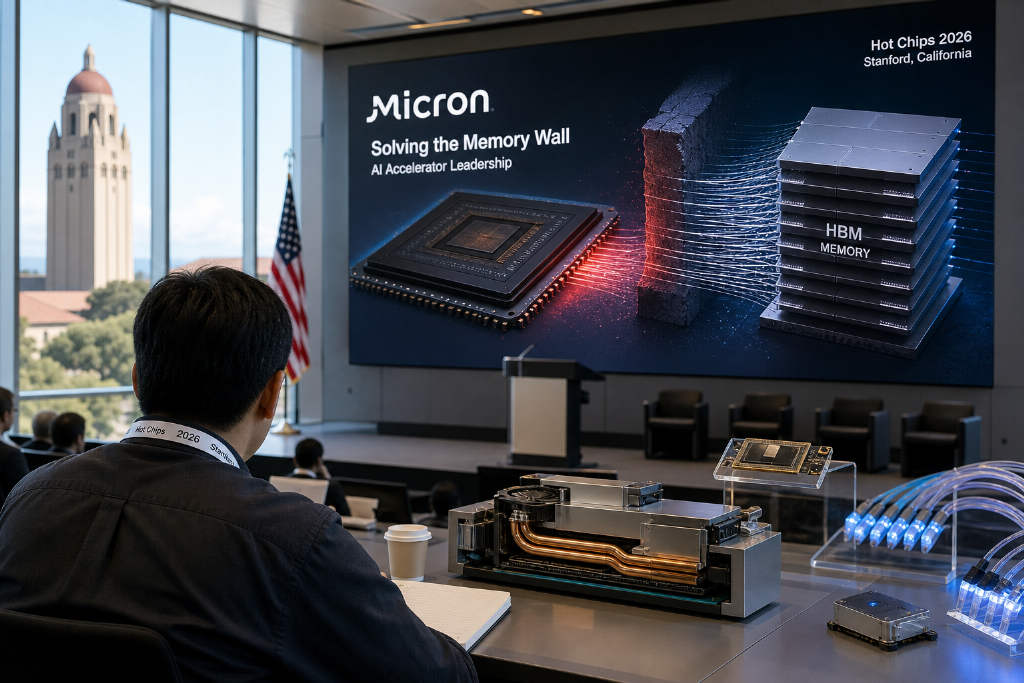
Micron said at Hot Chips 2026 that the industry’s memory wall is still intact and getting worse as AI systems scale. Speaking on Aug. 23 U.S. West Coast time at the semiconductor conference held at Stanford University, Micron HBM design architecture specialist Ragu Sriramaneni said AI accelerator compute performance is improving by about 3x every two years, while high-bandwidth memory, or HBM, is delivering less than 2x bandwidth growth over the same period.
Compute gains are outpacing memory bandwidth
Micron used the comparison to show how the gap between processing capability and data delivery keeps widening. The memory wall refers to a bottleneck in which compute chips advance faster than the memory systems feeding them. In Micron’s telling, AI has not eased that problem. It has made it more visible.
The company said that even if accelerator performance keeps moving higher, end-system results will still be constrained if data channels cannot keep up. That puts memory technology near the center of AI system performance limits.
Micron casts HBM as the link between compute and memory
Micron described HBM as the bridge connecting compute units and memory in AI systems. According to the company’s product-page definition cited in the report, HBM is a high-bandwidth memory technology built for AI and high-performance computing, using stacked DRAM dies to deliver more bandwidth and capacity within limited space.
As an example, Micron said a typical accelerator paired with eight 12-high HBM4 stacks could have a total memory die area more than eight times larger than the logic die area itself. HBM lifts bandwidth without sharply increasing package size because it integrates memory directly with the accelerator in a system-in-package, or SiP, rather than using traditional discrete slot-based modules.
From HBM3E to HBM4, Micron said both data rates and stack heights are moving up. It added that HBM3E has 128 channels per DRAM die, while HBM4 doubles that figure to 256.
Higher bandwidth comes with higher silicon cost and harder thermal work
Micron said the performance gain is expensive. At the same capacity, providing HBM3E-level performance requires total silicon area of about three times that of DDR5 once architecture choices, advanced packaging and manufacturing complexity are included.
The report linked that cost structure to the growing share of memory in AI system buildouts, and cited earlier reporting that HBM now accounts for more than 60% of the memory cost of a single AI chip.
Micron also pointed to reliability issues. In heterogeneous integration, chips and bulk materials are stressed by mismatched coefficients of thermal expansion. Starting with HBM3, ECC coverage is split across a system layer and a chip layer. As AI workloads rise and stacks get taller, cooling becomes a tougher engineering problem as well.
Micron says the next step is to blur the line between compute and memory
Micron’s conclusion was that the way past the memory wall will not come from a single chip improvement alone. The company said future systems will need to break down the boundary between compute and memory, embedding memory more deeply into the compute flow through SiP, optical interconnects and more advanced packaging such as CoWoS-L and CoWoS-R.
The report added that this direction carries implications for Taiwan’s supply chain because HBM depends heavily on advanced packaging and glass-substrate technologies, areas tied to the CoWoS packaging and testing capabilities of Taiwanese semiconductor companies. It also noted that AMD and NVIDIA have in recent years gradually shifted packaging demand to Taiwanese partners.
In Micron’s presentation at Hot Chips 2026, the memory roadmap pointed to an AI hardware race that is no longer only about raw compute. Memory and packaging are taking a larger role in the contest.