
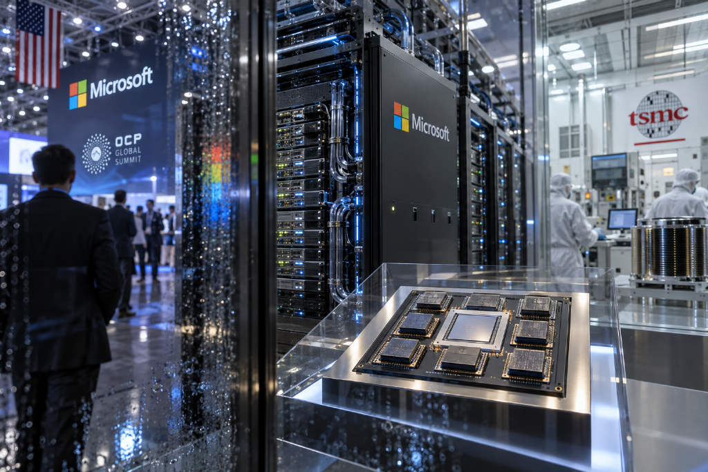
Microsoft (MSFT) introduced its third-generation in-house AI accelerator, Maia 300, at the Open Compute Project (OCP) Global Summit on Oct. 12 U.S. time. According to a report cited by ABMedia from Economic Daily News, the chip’s core compute die will use Taiwan Semiconductor Manufacturing Co.’s (TSMC, 2330) 2 nm-class N2P process, with large-scale deployment expected to begin in 2027.
Maia 300 moves Microsoft’s AI silicon onto TSMC’s N2P node
The report said early 2 nm production at TSMC had been driven mainly by flagship smartphone chips. Microsoft’s decision to move its in-house AI processor onto the node points to a broader customer mix, extending from mobile applications into cloud AI and data center workloads. ABMedia said that shift could add a new source of growth for TSMC’s advanced-node business next year.
First chiplet-based Maia design with eight HBM4 stacks
Based on specifications released by Microsoft, Maia 300 is the company’s first AI chip built on a chiplet architecture. Compute, memory control, and input/output functions are separated into different dies. The compute die uses TSMC’s N2P process, while the previous Maia 200 used a monolithic 3 nm design.
On memory, Maia 300 is equipped with eight HBM4 stacks for a total of 288GB, more than 30% above the 216GB in the prior generation. Power consumption is 950 watts per chip. A single rack can hold 96 accelerators, twice the Maia 200 level.
Microsoft said to be discussing capacity for more than 300,000 units
Microsoft has been pushing its in-house chip program to reduce reliance on outside suppliers such as Nvidia (NVDA). Citing The Information, ABMedia said Microsoft is in talks for capacity exceeding 300,000 Maia 300 units, with a long-term target that could reach 1 million units. Delivery is expected in 2027.
ABMedia also said Taiwan supply chain sources indicated Maia 300 will begin mass production this quarter, and that TSMC is stepping up capacity preparations. The report added that some market participants expect faster deployment of Microsoft’s in-house AI chips to support TSMC’s business.
TSMC expands 2 nm output across five fabs
To meet AI-driven demand, TSMC is set to ramp output from five 2 nm fabs this year, located in Hsinchu and Kaohsiung. The N2P process in the 2 nm family is also expected to enter mass production in the second half of this year.
TSMC said 2 nm capacity will post a compound annual growth rate of 70% from 2026 to 2028. Wafer output in the first year of 2 nm mass production is expected to be 45% higher than first-year 3 nm output in 2023.
Market estimates cited by ABMedia put TSMC’s monthly 2 nm capacity at about 90,000 to 100,000 wafers by the end of this year, rising to more than 110,000 wafers by the middle of next year. The report said some market watchers expect 2 nm revenue contribution in the second half of this year to approach 10% as smartphone and cloud AI customers both increase orders.