
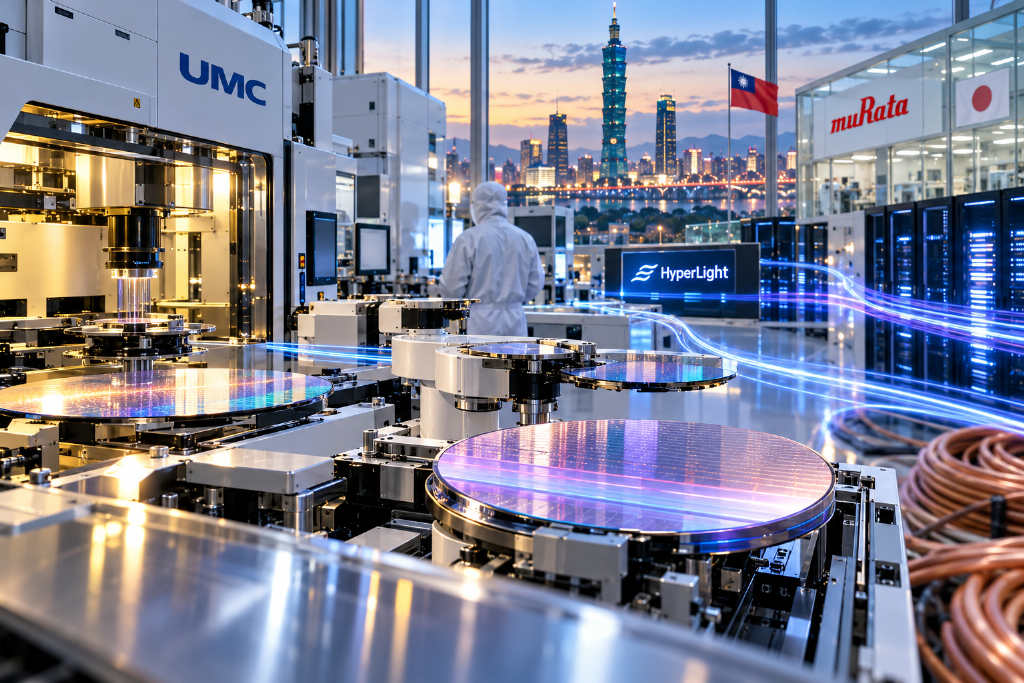
As AI clusters demand faster data movement, the limits of copper interconnects and conventional silicon photonic modulators are becoming harder to ignore. That has pushed industry attention toward TFLN, or thin-film lithium niobate, an older material being reworked for next-generation optical modulators.

Murata Manufacturing has laid out plans for a TFLN optical modulator and is targeting mass production in 2028. United Microelectronics Corp. (UMC) and its affiliate Lianying Photonics have also announced a partnership with HyperLight to manufacture a TFLN platform on 6-inch and 8-inch wafers. Across materials, components and foundry production, TFLN is moving out of the lab and into manufacturing lines.
What TFLN is
TFLN is made by slicing single-crystal lithium niobate (LiNbO₃) into films a few hundred nanometers thick, then bonding those films onto substrates such as silicon or quartz to form a lithium-niobate-on-insulator, or LNOI, structure. Its role is not to carry light itself. It is used to build optical modulators that encode electrical signals onto laser light.
The operating principle comes from the Pockels effect. When voltage is applied to lithium niobate, its refractive index changes almost instantly, allowing the intensity or phase of light to be controlled. That fast and linear response is the physical basis for TFLN’s high-speed transmission capability.
Why AI data centers are looking at TFLN
One of the most immediate bottlenecks in AI computing is how to move data efficiently. Executives from Marvell said at the AI Infra Summit that as per-lane speeds move from 224G to 448G, signal integrity over copper becomes a major constraint on link distance, making optical links more attractive for rack-to-rack connections.
At the same time, the industry is moving from 1.6T toward 3.2T, raising the bar for both modulator speed and power consumption. The main advantages highlighted for TFLN are:
- High bandwidth, supporting higher per-lane data rates.
- Low drive voltage, potentially close to CMOS voltage levels and helpful for reducing driver-side power use.
- Low optical loss, which improves signal quality.
Those characteristics make TFLN a candidate material for 1.6T and 3.2T optical modules, coherent transmission and CPO, or co-packaged optics.
Manufacturing remains the main hurdle
The biggest constraint on TFLN is scale. Lithium niobate is hard and difficult to etch, which is why the technology has largely remained inside research fabs. The thin films themselves also require precise and technically demanding ion-slicing processes.
Wafer supply is another variable. Earlier this year, the United States used a defense contract to support domestic TFLN wafer capacity and acknowledged that existing supply is still largely controlled by offshore sources. For TFLN to make its way into AI data centers, performance alone will not be enough. It also has to be manufactured in standard foundry environments with stable output and lower cost.
UMC and Murata are taking different routes
UMC: foundry capacity for scale-up
In March, UMC, Lianying Photonics and HyperLight announced a strategic partnership to manufacture HyperLight’s TFLN chiplet platform on 6-inch and 8-inch wafers.
Under that arrangement, HyperLight handles platform architecture design, while UMC and Lianying provide foundry capacity. Lianying had already worked with HyperLight to move TFLN into a customer-qualified 6-inch CMOS production line. UMC added 8-inch capacity to expand the platform’s scale.
The platform is aimed at short-reach pluggable modules for data centers, long-haul coherent modules and CPO applications. Hung Kuei-chun, senior vice president at UMC, said TFLN is becoming a key material for data center transmission above 1.6T.
Murata: control over materials and device processing
In June, Murata released its own CPO technology roadmap, covering optical modulators, package substrates and high-speed wiring, with a goal of integrating optical, electrical and thermal functions by 2032.
Within that roadmap, Murata expects to complete its first TFLN modulator samples in the fourth quarter of this year and move into mass production in 2028. Its targets are electro-optic bandwidth above 100 GHz and per-lane transmission speeds above 400 Gbps. Murata said it plans to build on the lithium niobate materials and process experience it developed through surface acoustic wave, or SAW, filters used in smartphones, and to keep control of both wafer and device processing in-house.
2027 to 2028 will be the key test window
TFLN’s outlook has drawn strong interest, but several variables remain unresolved. The list includes long production timelines, unstable yields and continued progress in competing modulator approaches such as silicon photonics.
The material has already shown enough technical advantages to stay in the running as an important next-step option. The real question now is whether it can be produced consistently and at lower cost. Sample deliveries and shipments in 2027 and 2028 are likely to be the clearest test of that path.