

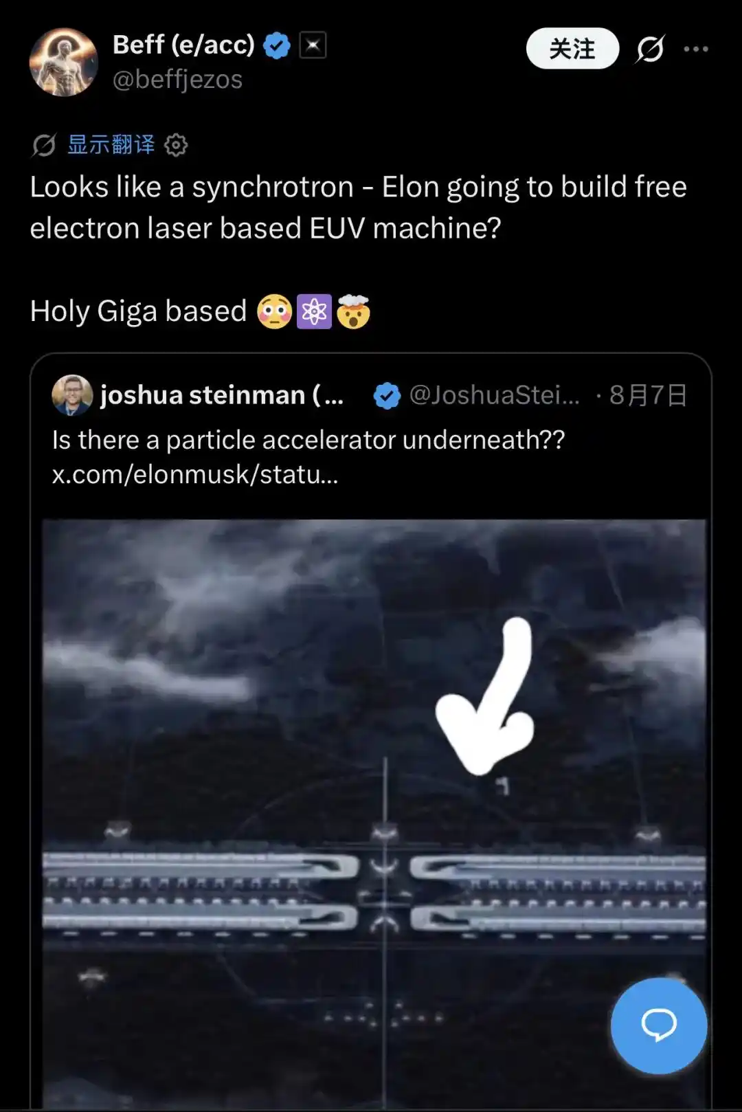
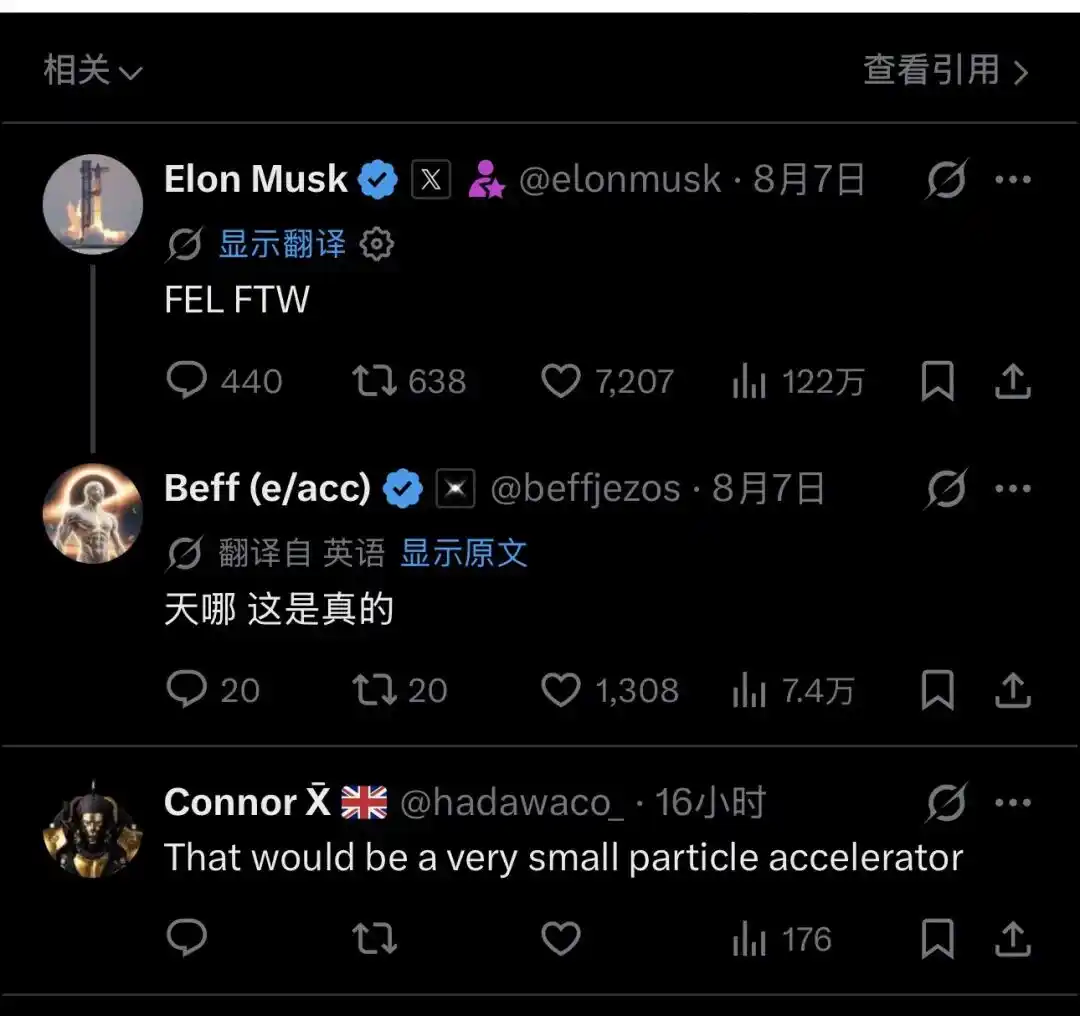
Speculation around TeraFab and a reply from Elon Musk has prompted renewed discussion about whether a free-electron laser, or FEL, could emerge as an alternative route for extreme ultraviolet lithography light sources.
The source article says plainly that this is still a guess, not confirmation of what Musk is actually building. Even so, it argues that the FEL route itself deserves a closer look.
FEL is not a new idea
Free-electron lasers and particle accelerators have existed for years. Companies, research institutions and universities have long operated accelerators to generate subatomic particles such as protons, neutrons and quarks for physics and other scientific work. FEL systems also have a long history. In the article’s framing, an FEL is essentially a high-power light source that uses electrons to generate light at different wavelengths, while a particle accelerator is the system that drives charged particles forward.
In principle, an FEL works by sending electrons moving at nearly the speed of light through a periodically changing magnetic field. The emitted laser wavelength is tied to the frequency of that periodic magnetic process. By changing the magnetic-field period or the incoming electron speed, the system can produce different wavelengths. That is why an FEL first needs a high-speed electron source operating close to light speed.
The article explains that only under those conditions can the radiation generated by the electrons’ transverse motion significantly affect the electrons themselves, causing nearby electrons to bunch together instead of remaining a uniform stream.
If each bunch contains N electrons, the combined radiated energy is no longer a simple linear sum. The article describes it as scaling with N squared, meaning the radiation becomes coherent and forms laser light. Linear accelerators are currently the most common high-speed electron source for this purpose, while synchrotron-radiation-based approaches also exist but are described in the article as lacking sufficient power.
Put simply, in an FEL, electrons move freely in vacuum at close to light speed and exchange energy with a co-propagating electromagnetic wave, producing a tunable beam that is amplified exponentially.
How the system is structured
High-energy electron beam
The process starts with a high-energy electron beam from a particle accelerator. A microwave amplifier accelerates electrons to near light speed. Using a 1 GeV beam as an example, the article says the electrons travel only one ten-millionth slower than light. Higher electron-beam energy translates into higher photon energy from the FEL.
Radiation from accelerated charge
Any charged particle that is accelerated emits light. The article cites bremsstrahlung as one example, where electrons strike a metal wall and rapidly decelerate, losing energy through radiation and heat.
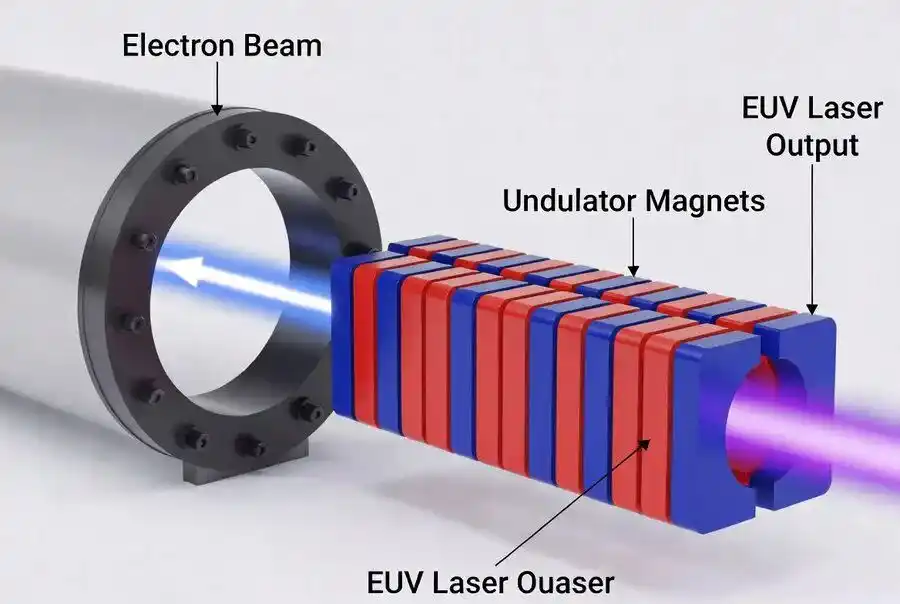
Bending magnets can create a related effect. If the beam is bent into a circular orbit, the result is a synchrotron-radiation source. If the beam is forced into a back-and-forth sinusoidal path, it becomes a wiggler or undulator source. Synchrotron and wiggler sources produce broader frequencies, while an undulator can, under specific conditions, enable laser emission from the passing electron beam.
Undulator
An undulator is built from periodically arranged magnets that make a high-energy electron beam oscillate along a sinusoidal path at a defined frequency. That controlled oscillation is the first step toward precise, tunable light. The undulator period, together with the beam energy, sets the output wavelength.
That is why some see FEL as a candidate to replace the light source used in EUV lithography.
Why it is being discussed as an EUV source candidate
Conventional EUV lithography uses 13.5 nm light because tin plasma can generate that band relatively efficiently.
FEL follows a different logic. By adjusting electron-beam energy, the undulator period and magnetic-field strength, the output wavelength can be changed. In theory, that range can stretch from soft X-rays through EUV and on to longer bands. The article compares conventional EUV to a fixed-focus cutting tool, while FEL is described more like an optical tool with an adjustable wavelength.
That is why some groups are trying to use FEL to break through current limits. The article names U.S. startup xLight as a supporter of this path and notes that former Intel CEO Pat Gelsinger is now xLight’s executive chairman.
In xLight’s setup, electrons are first injected into a particle accelerator and then enter the FEL. The company is quoted as saying: “FEL utilizes electrons from a particle accelerator and passes them through an undulator with a periodic magnetic field to generate a coherent, high-intensity beam of light.”
In simple terms, the article says the EUV light is generated in the accelerator. It is then sent through what is described as a photon-pipeline-like system from the accelerator equipment to the fab, and from there directed into a sub-fab area. Inside that lower-level facility are separate systems referred to as “switchyards” in the article’s description.
Based on xLight’s video, each of those stations is dedicated to one EUV tool in the fab above. During operation, the EUV light is delivered to each rotating station in the sub-fab area, where it is received and guided up to the EUV system on the fab floor, supplying power to the lithography tool.
Under that arrangement, the EUV tool itself does not contain an LPP source. Instead, EUV light is created in the particle accelerator and then transmitted to the fab tool. The article presents this as a simplified explanation of a more complex process.
xLight’s stated performance claims
The article says xLight’s FEL light source produces four times the power of current LPP systems. It quotes xLight as saying: “By providing up to 4x EUV power, fabs can optimize patterning improvement, increase productivity and yield, resulting in billions of dollars of additional annual revenue per scanner and reducing wafer cost by approximately 50%. In addition, a single xLight system can support up to 20 ASML systems and operate for up to 30 years, reducing capital and operating expenditures by more than 3x.”
The same article says xLight’s technology could theoretically be applied to low-NA EUV, high-NA EUV and even hyper-NA EUV. On the development side, it notes that ASML is working on 0.75 hyper-NA EUV technology aimed at a more distant future.
It then argues that TeraFab’s long, narrow facility design, together with Musk’s reply, suggests TeraFab may use a linear accelerator as the high-speed electron source for FEL. The article also notes that femtosecond free-electron X-ray lasers are already used in university laboratories to collect data for protein crystal diffraction.
To illustrate the difference, the article uses a simple comparison. If the light source in ASML’s EUV lithography systems is like an ordinary bulb, then an FEL-based EUV source is more like a highly efficient laser that can more easily generate output in the kilowatt to tens-of-kilowatts range, while also allowing the wavelength to be tuned.
By contrast, the article says ASML’s LPP EUV uses a fixed wavelength and has difficulty breaking through the 1 kW level. It also says LPP cannot match FEL in wavelength purity or coherence. If such a system could be built, the article argues, it could improve both lithography speed and patterning quality.
On energy use, the piece gives another comparison. It says ASML’s LPP setup needs about 4.4 MW of electricity to produce 1 kW of usable EUV, for an overall efficiency on the order of 0.05%. An advanced energy-recovery FEL, or ERL-FEL, by contrast, would need about 0.7 MW to produce 1 kW of EUV, or about six times the efficiency. The article adds that better superconducting materials could raise that further in the future.
Better source physics does not mean immediate manufacturing fit
The article also makes a clear distinction between source performance and production readiness. On source physics alone, FEL is stronger. That does not mean it is already the more advanced option for industrial lithography, because EUV manufacturing needs more than just a beam at 13.5 nm.
It also needs high power, high stability, high repetition rate, high reliability, very low cost, extremely high uptime and compatibility with reflective optical systems.
ASML’s current EUV source has gone through years of engineering and now sits inside a complete industrial system. FEL, by comparison, usually requires large electron accelerators, undulators, vacuum systems and beam-control systems, which makes the equipment physically large and expensive.
So the article draws a split conclusion. From the standpoint of source physics, FEL is clearly stronger and more flexible. From the standpoint of semiconductor mass-production engineering, today’s mature EUV source is still better suited to fabs. The possible long-term value of FEL is that it could push lithography away from a fixed 13.5 nm source and toward more flexible short-wavelength options.
The article points to possible future exploration at 6.x nm, 5.x nm and even shorter wavelengths, where FEL’s tunability, coherence and high peak brightness could become especially attractive.
But the shorter the wavelength gets, the harder the surrounding problems become. The article specifically mentions optics, masks, photoresists, reflectivity, photon scattering and vacuum systems.
FEL is not the only path under discussion
In the article’s view, the real significance of FEL may not be limited to replacing an EUV source. It may instead offer a completely different route to a high-brightness short-wavelength source.
It also mentions high harmonic generation, or HHG, discharge-produced plasma, or DPP, and synchrotron radiation as other routes under discussion. Its comparison is straightforward: LPP is mature and ready for volume production, FEL is defined by high brightness, high coherence and tunable wavelength, while HHG has miniaturization potential. The key competition, it says, will be whether any of these approaches can balance power, efficiency, stability and cost at shorter wavelengths.
The article ends by noting that all of these options still face major challenges, and no firm timeline has been set.
The source piece was originally published by the WeChat public account “Semiconductor Industry Watch” (ID: icbank) and credited to its editorial team.