
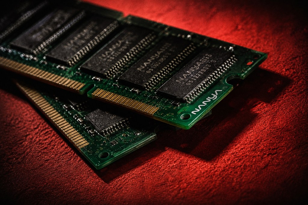
As AI workloads move from cloud training to inference, Nanya Technology argues that high bandwidth memory is no longer the most practical answer for every use case. Wu Chih-hsiang, the company’s senior vice president, said at the Industrial Technology Research Institute’s “Semiconductor and AI Computing Sustainable Competitiveness Forum” yesterday that HBM’s built-in constraints in power consumption and I/O architecture make it ill-suited for edge inference scenarios. Nanya is now pushing what it calls custom UWIO DRAM with 3D IC stacking, with its new Taishan plant set as the core of that expansion and mass production targeted as early as the beginning of next year.
Inference workloads are changing memory priorities
For the past several years, HBM has been a key memory technology behind large-scale AI model training and a standard feature of high-performance computing systems. Wu said that dynamic is starting to change as AI development shifts away from large cloud training clusters and toward inference running on end-user devices.
In edge inference, devices must handle large volumes of conversation history and KV cache generated on the user side. That raises pressure on both memory bandwidth and power efficiency. Wu said HBM is constrained by a limited number of I/O pins and relatively high energy use, making it a poor fit for products that prioritize response time and power efficiency, including AI PCs, smartphones, and portable devices.
In his framing, HBM solved a training-era problem. The inference era needs a different memory design.
Custom UWIO DRAM and WoW stacking are Nanya’s answer
To target that gap, Nanya is building around custom UWIO DRAM combined with Wafer-on-Wafer, or WoW, 3D IC stacking. The approach allows DRAM to sit directly on top of CPU or ASIC logic chips, removing some of the signal loss and latency that come with conventional package interconnects.
Wu said the architecture offers a clear performance advantage. Bandwidth can increase by 5x to 10x compared with traditional designs, while per-bit energy consumption falls to between one-third and one-tenth of HBM. For edge devices, that means lower thermal design power without giving up performance, directly addressing a central constraint in AI endpoint hardware.
AI PCs are driving a sharp increase in memory demand
Nanya also linked its strategic shift to expected demand growth. Using AI PCs as an example, the company said memory capacity per unit has climbed from 16GB to 128GB. With annual global shipments in the hundreds of millions of units, DRAM demand is expected to enter what the source described as an exponential expansion cycle.
To prepare for that demand, Nanya said it is advancing both process technology and product lines at the same time. Its main 16nm, or 1B-generation, products have expanded to more than 10 items. At the same time, the company is developing three more advanced generations — 1C, 1D, and 1E — in parallel. The source said this shows Nanya is trying to accelerate its roadmap and shorten the gap between generations so it can track market demand more closely.
Taishan fab is central to the production plan
On capacity, Nanya’s new wafer fab in Taishan, New Taipei City, is described as the company’s most important move. Total planned investment in the site stands at NT$500 billion. The fab is expected to adopt EUV lithography equipment, and capital expenditure next year is initially estimated at more than NT$200 billion. The company plans to bring the facility into production at the start of next year, which the source said would help narrow the gap between Nanya and major international players such as Micron and SK hynix in both process technology and scale.
Process shrink and sustainability targets are moving together
Wu said Nanya does not see technology upgrades and sustainability goals as competing priorities. He gave one example: power consumption for products built on the 1C process is 34% lower than for products based on the 1A process.
On the operations side, Nanya said its sites are now equipped 100% with local scrubber exhaust gas treatment systems and AMAT i-System smart control systems, giving it a greenhouse gas reduction efficiency of 94%. Through its ISO 50001 energy management system, the company has also maintained annual electricity savings of 8% to 9% for several consecutive years. The source described that as a competitive advantage at a time when sustainability requirements across customer supply chains are becoming stricter.