


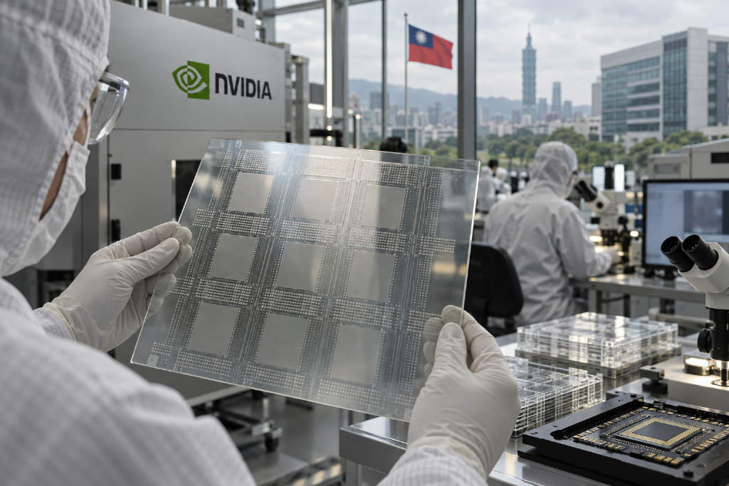
Glass substrates are increasingly being viewed as a possible next step in advanced packaging as AI chips grow larger and their structures become more complex. Korean outlet KIPOST recently reported that NVIDIA is evaluating the technology for next-generation AI chip packaging and has asked substrate makers in South Korea, Japan, and Taiwan to complete development within two years, with the aim of bringing it in before 2028.
The report quickly put Taiwan’s display and glass supply chain in focus. Even so, industry participants cautioned that manufacturing yield and customer qualification still stand as the key barriers before glass substrates can move into large-scale commercial use.
NVIDIA reportedly steps up supplier talks and sets a two-year development window
According to the Seoul Economic Daily, NVIDIA is working with several partners to explore glass substrates as part of an effort to improve AI semiconductor performance. German equipment maker SCHMID was named as one of the companies involved. A more recent report said NVIDIA asked substrate suppliers in South Korea, Japan, and Taiwan to complete related development work within two years, creating a path for adoption before 2028.
The same report said NVIDIA is not only speaking with individual suppliers but is also looking to push coordinated development across the broader supply chain. It added that NVIDIA CEO Jensen Huang and SK Group Chairman Chey Tae-won discussed cooperation on next-generation semiconductor technologies, including glass substrates.
South Korean companies are moving as well. ChainNews previously reported that SKC had pushed back its mass-production schedule for glass substrates to 2027 while seeking to complete final verification before year-end. Another report said Samsung Electro-Mechanics, SKC, and LG were targeting 2027 to 2028 for volume ramp-up, while BOE had also entered the field.
AUO builds out TGV and RDL lines and showcases a glass-core substrate with Corning
Within Taiwan’s supply chain, AUO has drawn particular attention. The Liberty Times reported that the company is using its existing strengths in large-size glass processing, precision metallization, and redistribution layer, or RDL, capabilities to expand into advanced semiconductor packaging. It is also planning pilot lines for through-glass vias, or TGV, RDL, and glass-core technologies.
Chairman Paul Peng said in July that the related projects had been included in the company’s NT$8.6 billion capital expenditure plan. He also said glass-core technology would likely need another two to three years before reaching a more mature stage.
At SEMICON Taiwan 2026, AUO and Corning jointly presented a 510 × 515 mm glass-core substrate. The product combines Corning’s semiconductor-grade glass with AUO’s RDL process and is designed to meet the needs of increasingly large AI server chips, especially in high-density interconnects and low-loss transmission.
Innolux targets panel-level packaging with a 620 × 670 mm format
Innolux, ticker 3481, is continuing to develop TGV technology while running customer validation. Business Today reported that Chairman James Hung said the company is working with customers on product development and verification, and that the market broadly expects glass substrates to reach mass production as early as 2028.
To strengthen its panel-level packaging research, Innolux is using a 620 × 670 mm panel format. Commercial Times described that as the industry’s largest size. The platform supports panel-level packaging with multi-layer RDL and advanced packaging applications similar to CoPoS-L.
More Taiwan suppliers join the push
Beyond the two major panel makers, other Taiwan companies are moving into the area. Commercial Times said glass processor GTOC is developing thermoforming technology for TGV and substrate applications and has already filed related patents.
Touch panel maker TPK, ticker 3673, began researching TGV about two years ago by drawing on its existing glass-processing experience. Its pilot line in Zhongli started operating in early September, and the company is also working with semiconductor packaging and testing firms.
Whether 2028 is achievable still depends on yield and qualification
Despite the growing activity, glass substrates are still some distance from large-scale mass production. Industry participants said the biggest challenges remain process yield and customer qualification.
There is another point to keep in view. The claims that NVIDIA wants development completed within two years and hopes to introduce the technology before 2028 currently come mainly from media reports, and NVIDIA has not publicly confirmed them. AUO itself has also said that glass-core technology still needs another two to three years to become more mature.
That leaves 2028 as an optimistic target rather than a fixed timetable. The actual schedule will depend on each company’s technical progress and the outcome of customer verification.