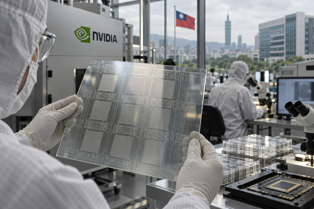
NVIDIA2026-10-01 09:48:35NVIDIA said to set a two-year glass substrate timeline as Taiwan suppliers aim for 2028 adoptionReports from Korean and Taiwanese media say NVIDIA is evaluating glass substrates for next-generation AI chip packaging and has asked substrate makers in South Korea, Japan, and Taiwan to complete development within two years, with a target of introducing the technology before 2028. The move has drawn attention to Taiwan’s display and glass supply chain, where AUO, Innolux, and other companies are building capabilities around through-glass vias, redistribution layers, and glass-core substrates. AUO has folded related work into an NT$8.6 billion capital expenditure plan and, together with Corning, showcased a 510 × 515 mm glass-core substrate at SEMICON Taiwan 2026. Innolux is also pushing customer validation and using a 620 × 670 mm panel format that local media described as the industry’s largest. At the same time, local glass processing and touch-panel companies are joining the field. Even so, the commercialization path is still uncertain. Industry participants cited in the report said manufacturing yield and customer qualification remain the main hurdles, and NVIDIA has not publicly confirmed the reported two-year development request or the 2028 introduction schedule.800
Intel2026-09-21 08:12:25Intel rises more than 5% in premarket trading after Micro LED packaging plan with AUOIntel shares rose more than 5% in U.S. premarket trading, according to data from MSX.COM, in a move highlighted by Odaily. The gain came after the company had earlier announced a partnership with AUO to develop advanced Micro LED packaging. The stated target is the CPO market and high-density computing integration. The update was brief and focused on the immediate price move and the related corporate announcement. No additional pricing details, timeline, or financial terms were disclosed in the source. The report tied the premarket advance to Intel’s previously announced plan to work with AUO on Micro LED advanced packaging aimed at CPO and dense computing applications.550
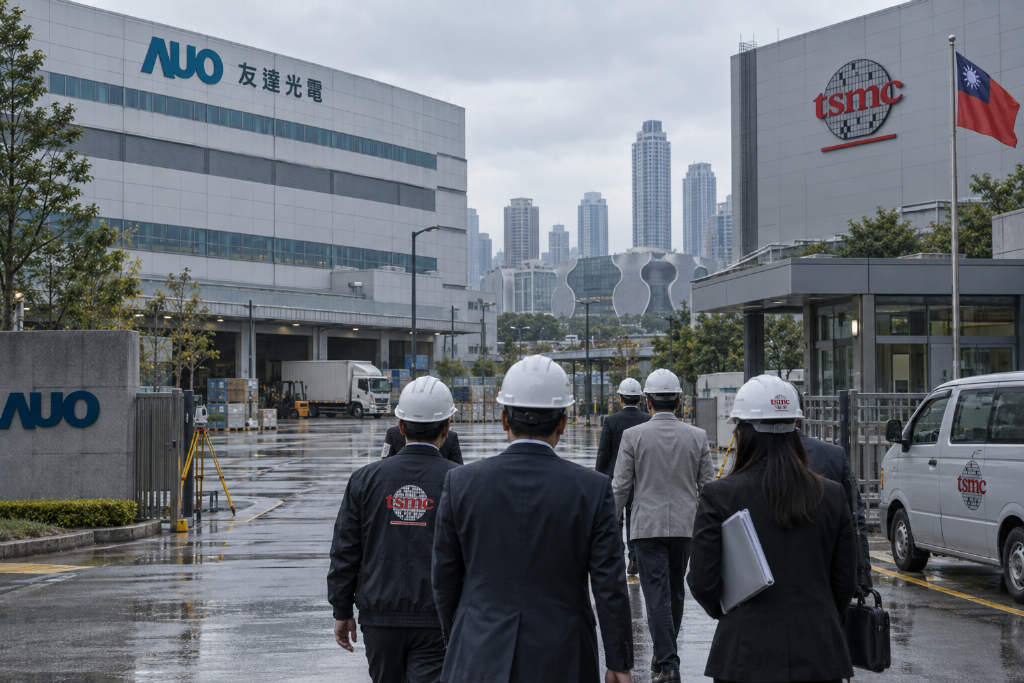
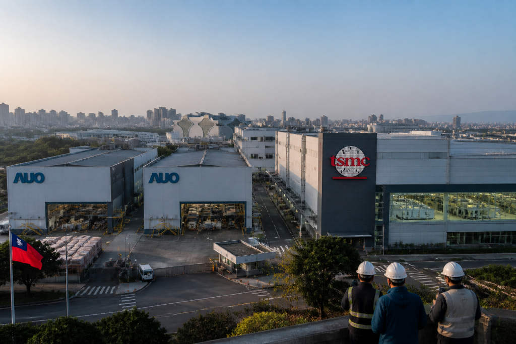
AUO2026-09-21 05:39:53AUO recoups NT$34.7 billion from three plant sales as TSMC is said to inspect two CTSP fabs and discuss technical cooperationAUO has completed three asset monetization deals this year, bringing in about NT$34.7 billion, according to a report cited in the source material. The transactions include the sale of a Gen 5 fab in Huaya Technology Park to Quanta for NT$19.7 billion, a Gen 5 color filter plant in Kaohsiung’s Luzhu Science Park to ASE for NT$6.3 billion, and the sale of its Singapore AFPD facility to Western Digital for about S$350 million, or roughly NT$8.753 billion. The latest market talk says Taiwan Semiconductor Manufacturing Co. has visited AUO’s L5C and L7A plants in the Central Taiwan Science Park. The discussions are said to cover not only the two facilities but also possible technical cooperation. The report says the two CTSP sites already have cleanroom, power, ultrapure water, and exhaust treatment infrastructure in place, with L7A next to TSMC’s existing CTSP operations and L5C adjacent to L7A. The report also links AUO’s process strengths in large-area substrate thin-film manufacturing, TFT Array production, precision alignment, and uniformity control to possible FOPLP development. Even if talks move ahead smoothly, outside estimates cited in the report say a formal agreement and closing would likely not come before the second half of next year.810
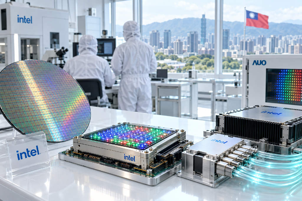
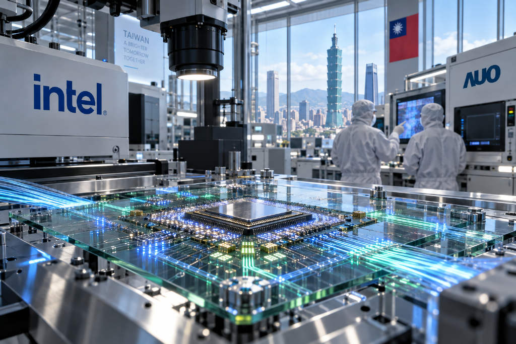
Intel2026-09-21 03:18:45Intel Said to Be in Talks With AUO on Micro LED Substrate Packaging for CPOIndustry sources say Intel has moved into advanced Micro LED substrate packaging and is in talks with AUO, one of Taiwan’s deepest Micro LED technology players, on a joint push into co-packaged optics, or CPO, and high-density compute chip integration. The report links the move to Intel’s broader packaging strategy, which already includes its EMIB technology and work around glass substrates. The report also points to Intel’s recently disclosed U.S. patent, "IC Package with Micro LEDs," as a window into that direction. The patent describes a structure in which a semiconductor die is at least partly embedded in a glass substrate with through-glass vias, or TGVs, providing electrical connections that can power Micro LEDs. According to the report, the design could support chip-status visualization, customized lighting effects, and in-situ optoelectronic testing during packaging without extra external components. AUO is seen as a logical counterpart because it has built a technology roadmap spanning Micro LED CPO, glass substrates, redistribution layers, and optical interconnects. AUO Chairman Paul Peng has previously said the company has established positions in advanced packaging and glass substrates and is co-developing projects with partners, though he did not name them because of confidentiality agreements.630
TSMC2026-08-24 02:01:13Report says TSMC may spend over NT$30 billion to buy two AUO plants near its Central Taiwan Science Park siteTSMC is rumored to be considering a purchase of two older-generation AUO display plants near its operations in the Central Taiwan Science Park, according to a report cited by ChainCatcher from Commercial Times. The reported deal value is more than NT$30 billion, and the facilities — AUO’s L7 and L5C plants — would be kept as space for large-format packaging development tied to CoPoS and FOPLP. People familiar with the matter, as cited in the report, said TSMC has already completed on-site due diligence. AUO is said to be planning to prioritize the disposal of the two factory sites, with a board submission target in October and a goal of finishing production-line relocation and clearing the facilities by the end of the first quarter next year. Neither TSMC nor AUO has confirmed the transaction. The report also described a broader buildout in central Taiwan. Industry sources said TSMC is extending its footprint from A14 process technology and advanced packaging to the COUPE silicon photonics platform, while existing and planned sites in the park include Fab 15A, Fab 25 and the AP5 advanced packaging and testing facility. On the optics side, Largan has recently acquired land and factory properties in Taichung, with the market reading those moves as preparation for CPO-related volume production.1630
TSMC2026-08-10 04:22:46TSMC pushes CoPoS and COUPE as AUO group companies line up around CPOTaiwan Semiconductor Manufacturing Co. is accelerating work on its CoPoS and COUPE silicon photonics technologies, while AUO-linked companies Epistar, Tyntek and LandMark Optoelectronics are assembling around the co-packaged optics, or CPO, theme, according to ABMedia. The report says the group is positioning itself across light emission, sensing and packaging as suppliers look for an early foothold in next-generation advanced packaging led by TSMC. ABMedia describes CoPoS as a packaging approach that replaces the traditional silicon interposer with a very large glass substrate, expanding the area available for integrating multiple high-performance GPUs and ASICs into a single package. But the report also notes that higher chip density intensifies heat and power problems in ultra-high-compute environments, where conventional electrical transmission and copper interconnects are approaching physical limits. Against that backdrop, CPO is being framed as a route to move part of the interconnect from electrical to optical signaling by integrating optical transceivers directly into the package. Economic Daily News, cited in the report, says AUO is handling packaging integration and testing, while Epistar, Tyntek and LandMark each focus on different optical components. Market observers cited by ABMedia expect the group’s validation work to convert into orders and revenue as TSMC’s CoPoS ecosystem moves toward volume ramp-up.2470