
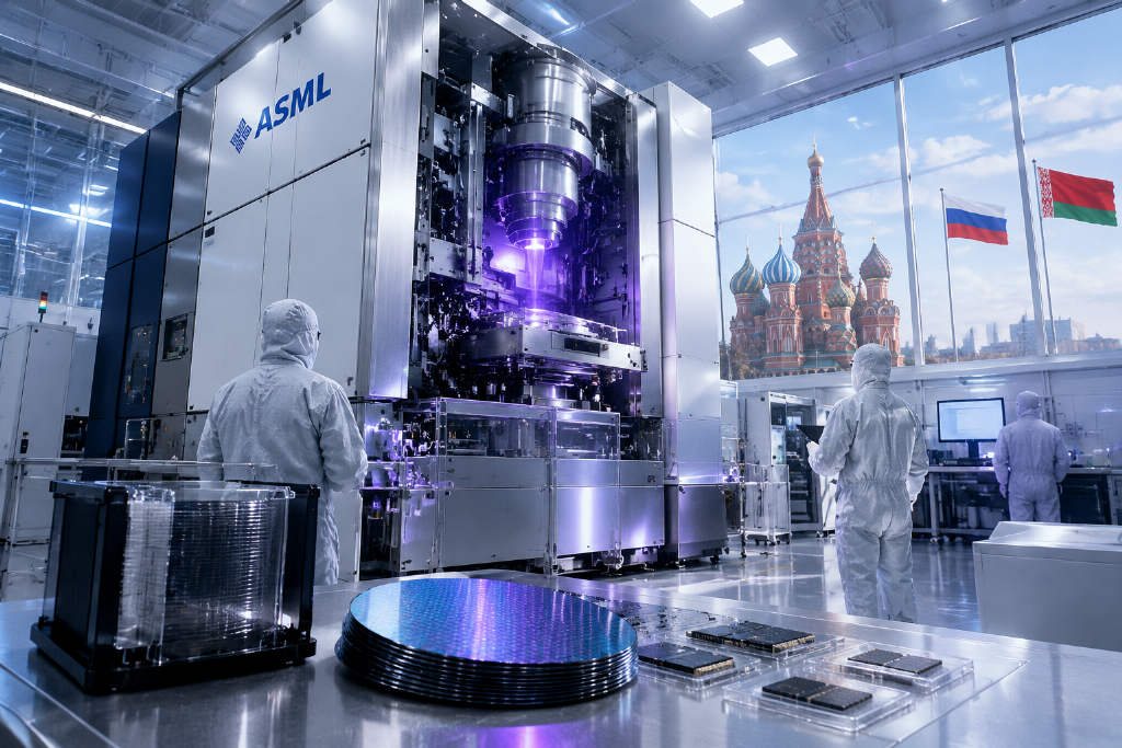
Russia and Belarus have built a 130 nm lithography prototype, and the domestically developed excimer laser for the system has completed testing, according to remarks by Russian First Deputy Prime Minister Denis Manturov at a microelectronics forum in September 2026. Manturov said full-machine acceptance is scheduled to start this autumn and end by the close of the year.
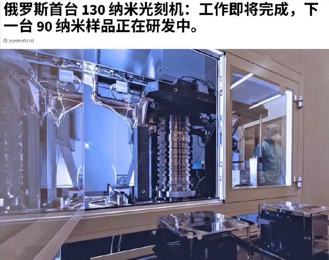
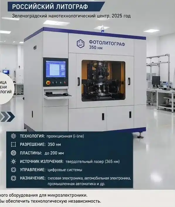
Before this, Russia had already introduced a 350 nm lithography tool. The report describes the move from that system to a 130 nm prototype within a matter of months as a major step for the country’s semiconductor equipment sector.
What the 130 nm tool is meant to do
The article places the machine in the mature-node segment of chip production. At the top end of lithography sits extreme ultraviolet, or EUV, which uses a 13.5 nm light source for sub-7 nm logic chips. Below that is deep ultraviolet, or DUV, using 248 nm KrF or 193 nm ArF light sources for processes ranging from 28 nm to 90 nm. Lower down are i-line systems and broad deep-ultraviolet exposure tools used for mature processes and power devices.
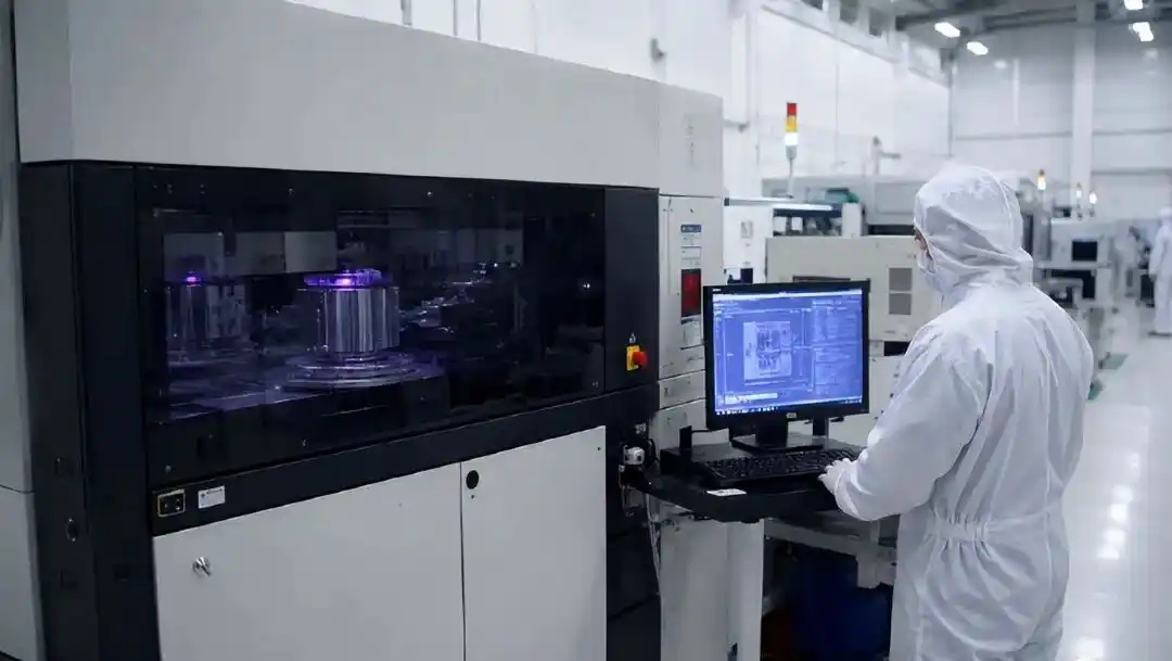
Russia’s 130 nm machine uses a 248 nm KrF excimer laser. The report notes that 130 nm is an old process node by current standards and points out that Intel’s Pentium 4 used the same node in 2002. Still, it argues that 130 nm remains useful in automotive electronics, industrial control, sensors, power devices, and military chips, where reliability and stable supply matter more than leading-edge scaling.
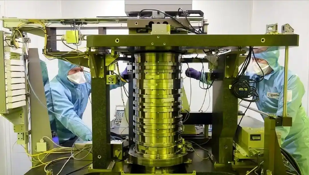
The article says Russia is not trying to build smartphone processors with this machine. Instead, it links the tool to products such as gyroscope chips used in missiles, avionics chips for the Su-57, and control chips for the S-400, arguing that 130 nm is sufficient for those uses and that domestic production became necessary after Western supply cutoffs.
The excimer laser is presented as the core breakthrough
Manturov repeatedly stressed the excimer laser in his remarks, according to the report. It says the minimum feature size a lithography system can print depends in part on the lens assembly and in part on the wavelength of the light source. For 248 nm KrF excimer lasers, the article says only three suppliers had previously been able to mass-produce them reliably: U.S.-based Cymer, later acquired by ASML, Japan’s Gigaphoton, and special versions from Germany’s Trumpf.
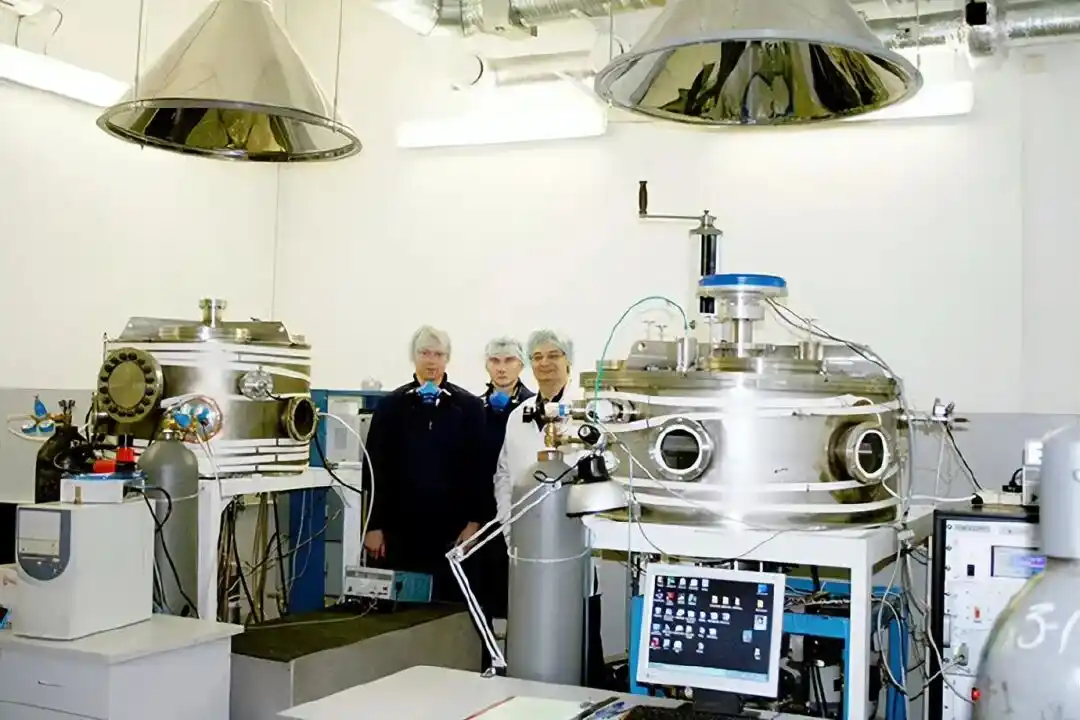
The report adds that the Lebedev Physical Institute of the Russian Academy of Sciences has worked on excimer lasers since the Soviet era. Even so, it draws a sharp line between laboratory research and industrial deployment, arguing that lighting a laser in a lab is very different from building a source that can run continuously for tens of thousands of hours inside a lithography system. In that framing, the real technical value of the new machine lies in moving the excimer laser from the lab to the production line. The article says that even if a DUV scanner could be obtained, a failed light source still left users dependent on U.S. or Japanese service providers.
Sanctions and the rebuilding of a Soviet-era base
The report traces Russia’s microelectronics decline over the three decades after the Soviet Union collapsed. It says factories aged, engineers moved to Israel and Germany, and the main process node in Russian fabs remained at 65 nm, around 15 years behind the United States.
After the first round of sanctions following Crimea in 2014, the article says Russia could still buy used DUV tools from the Netherlands. After the second round of sanctions in 2022, ASML halted spare parts and maintenance, TSMC canceled foundry orders from Russian design companies, and Synopsys and Cadence cut off EDA software licenses. The report says Russia’s response was to try to rebuild each broken link one by one.
Belarus is described as a key part of that effort. During the Soviet period, Minsk was a center of optical industry, and Planar, the Minsk-based optoelectronics manufacturer, had produced large amounts of lithography equipment and masks. After the Soviet breakup, that industrial base also declined, but the engineering teams and technical archives remained. The article says Russia brought materials and funding while Belarus contributed optical engineering talent, effectively reassembling a lithography foundation that had once been split across two Soviet republics.
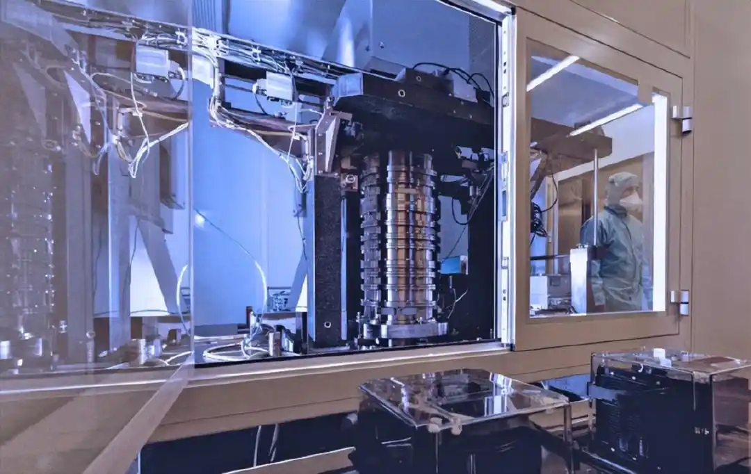
The roadmap points to 28 nm and then EUV
The roadmap cited from the Russian Academy of Sciences calls for 65 nm to 40 nm tools in 2026, 28 nm by 2032, and sub-10 nm EUV by 2036.
The article says the first two stages are not especially surprising because 28 nm can be produced with 193 nm ArF immersion DUV combined with multiple patterning. The more striking target is the EUV step.
ASML’s EUV systems use a 13.5 nm light source generated by firing a laser at tin droplets to create a plasma that emits EUV radiation, a setup known as laser-produced plasma, or LPP. The report says ASML spent 20 years and tens of billions of euros on that route, while yield and lifetime issues are still being refined.
Russia’s roadmap, by contrast, refers to an 11.2 nm laser source using a xenon laser instead of tin droplets. The article describes this as a different technical path. It says xenon excimer lasers have worked in laboratory EUV experiments, but no one has industrialized them at scale because conversion efficiency is low, lamp life is short, and power remains limited. The report argues that Russia chose this route not because it is better than the tin-droplet approach, but because it has a Soviet-era base in excimer laser research, while the tin-droplet LPP route is heavily covered by patents associated with ASML and Cymer.
The hardest constraints may sit outside the scanner
The article says lithography is only the most visible part of the semiconductor chain. To run a tool in a fab, the broader stack still requires photoresists, high-purity quartz glass, masks, CMP slurry, specialty gases, EDA software, and process engineers.
According to the report, Russia says it mastered 60 critical materials over the past three years and plans to add another 60 by 2029. It identifies EDA software as the more difficult bottleneck. Synopsys and Cadence dominate global digital chip design tools, while open-source options such as KLayout and Magic cannot replace them in analog design and advanced nodes. The article says Russia is pursuing in-house EDA development and produced a prototype in 2024, but it remains far from production-ready.
Talent is presented as another weak point. The report says the generation of optical and laser engineers trained in the Soviet era is now more than 60 years old on average. Younger microelectronics graduates, it says, often prefer jobs at Yandex in Moscow or move to Europe, leaving too few people in factories. The article argues that building a lithography machine is only the start; the systems must also be iterated, maintained, and repaired over time.
A mature-node tool, but a meaningful first step
The report concludes that the 130 nm machine is not advanced in the context of the current global semiconductor map. What it does show, in the article’s view, is that a country under severe sanctions can still rebuild a lithography supply chain from scratch in technical terms. It draws a line between mature-node manufacturing and the leading edge, saying 130 nm does not require EUV, 193 nm immersion, or the most advanced optics. What it does require is the reconstruction of many smaller links across materials, light sources, optics, and precision mechanics.
The article also says China spent 10 years building related capabilities, while Russia is now being pushed to rebuild under sanctions. It says the two face similar obstacles, including light sources, lenses, stages, photoresists, masks, and EDA.
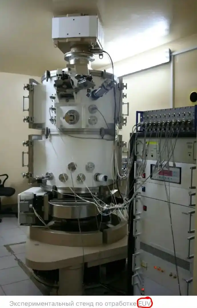
It adds that Russia’s accumulated work in excimer lasers, including the legacy of the Lebedev Institute and the Ioffe Institute, gives it a real technical base. If the 11.2 nm xenon route were to work by 2036, the report says, it would amount to a different technology tree from the one ASML built over 20 years and more than $100 billion. Whether Russia can actually reach 28 nm and then sub-10 nm will depend on whether it can close gaps in materials, talent, and EDA over the next decade.
The article ends on what it calls the hardest first step: a KrF excimer lamp that had previously been made only by suppliers in the United States and Japan can now be lit by Russian engineers themselves.
The piece was originally published on the WeChat public account Redian Weiping, written by Wang Xinxi, and republished by MarsBit.