

SanDisk and SK hynix are pushing a new way to use NAND Flash in AI systems, arguing that the technology better known from USB drives and SD cards could help ease memory pressure in large-model inference.
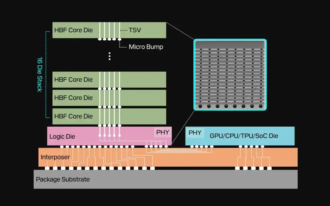
The concept, described by IEEE Spectrum, is called High Bandwidth Flash, or HBF. It takes the advanced packaging and die-stacking approach used in High Bandwidth Memory and applies it to NAND Flash, with the goal of turning flash from a storage-only medium into part of the high-speed data supply path for AI inference.
According to SanDisk’s public material, HBF is expected to stack as many as 16 NAND Flash chips, with a target capacity of up to 512GB per stack and read bandwidth of up to 1.6TB/s. The company’s roadmap for second- and third-generation products points to 2TB/s and 3.2TB/s, respectively.
Those figures still trail top-end HBM, but they are far removed from the conventional view of flash as slow storage. The key point is that HBF is not trying to make a single flash die dramatically faster on its own. It is trying to raise aggregate read bandwidth by combining multiple NAND dies through 3D packaging and vertical stacking.
Why flash can make sense for AI after all
The obvious objection is speed. Flash is widely associated with slow writes, which makes it seem ill-suited for AI workloads. Jim Handy, general director at semiconductor market research firm Objective Analysis, told IEEE Spectrum that many people have the same initial reaction: how could this work if flash is so slow?

The answer lies in where flash is slow. NAND Flash stores data through charges in floating-gate transistors and organizes information in blocks and pages. That design gives it non-volatile behavior, so data remains intact without the continuous refresh required by DRAM. It also brings high density and low cost. The tradeoff is write speed, because moving charge into and out of the insulated gate is much slower than charging and discharging a capacitor.
That is why flash has long been a poor comparison with DRAM or HBM in traditional computing discussions. But the picture changes if the focus is read performance rather than write behavior. Under the latest ONFI 6.0 flash interface standard, a single die can theoretically reach up to 4.8GB/s.
In isolation, that number is not especially high. A single DDR5 DIMM can reach up to 70.4GB/s, while an HBM4E stack can go as high as 3.6TB/s. The article notes that the gap between HBM4E and a single NAND Flash chip is roughly on the order of 750x. HBF is meant to narrow that gap at the system level by stacking many flash dies together.
Hoshik Kim, senior vice president of memory systems research at SK hynix, told IEEE Spectrum: "By applying advanced 3D packaging and vertical stacking technology to NAND flash, HBF can deliver bandwidth far beyond standard NVMe storage." Much as HBM stacks DRAM dies, HBF stacks NAND dies to create a denser and faster flash layer.
Inference, not training, is the target
The most practical use case for HBF is not model training. It is inference.
Training and inference put very different demands on memory. Training requires constant reading of weights, error calculation, and repeated weight updates through backpropagation. That workload involves heavy reads and heavy writes, which is a poor match for flash because write speed is slow and endurance management becomes an issue.
Inference looks different. Once a model is trained, its weights are largely fixed. The system mostly needs to read those large weights quickly rather than rewrite them over and over again. That makes static, read-heavy data a much more natural fit for HBF.
Kim said that in inference environments, "massive, read-intensive data such as static multi-billion-parameter model weights or precomputed KV cache can be safely placed in the HBF tier." In that setup, expensive and capacity-constrained HBM can be reserved for the fastest temporary working set, while HBF holds large parameter sets that rarely change.
That effectively adds a large-capacity, near-read-only pool to the AI memory hierarchy. HBM would continue to handle the most urgent and most frequently exchanged data. HBF would store very large but mostly static model parameters. Lower-speed, lower-cost data would remain on SSDs or other forms of storage.
What 512GB per stack and 1.6TB/s could change
SanDisk’s first-generation HBF target of up to 512GB and up to 1.6TB/s matters because it aims for a middle ground on capacity, bandwidth, and cost.
HBM is extremely fast, but it is expensive and limited in capacity. HBF would be slower, but it could offer larger capacity at a lower cost per unit. That means AI servers may not need to place every model weight in HBM during inference. Data that is colder, more static, and read much more often than it is written could sit in HBF instead.
The article outlines several possible benefits from that approach:
- easing HBM capacity bottlenecks,
- reducing the need to add more accelerator cards just to fit a model,
- lowering total inference system cost and power consumption.
Kim framed HBF and HBM as complementary rather than competing technologies. He said HBF could relieve the severe capacity bottleneck facing HBM without sacrificing data supply speed, potentially reducing the number of accelerators required to run large-scale models. He also said the approach could improve energy efficiency and lower costs, helping data centers expand AI inference hardware at larger scale.

A response to looming supply pressure
The timing also matters. On July 11 Beijing time, SK hynix CEO Kwak Noh-Jung said publicly on the day of the company’s Nasdaq debut that the global memory industry is expected to face its worst-ever supply shortage in 2027. The statement quickly drew attention from both capital markets and the broader industry.
Against that backdrop, the HBF effort from SK hynix and SanDisk can also be read as an attempt to create another technical answer to tightening memory supply. Large-model inference is already constrained by more than compute alone. Capacity limits, bandwidth limits, power consumption, and deployment cost are all rising at once. In many cases, the problem is not that a GPU cannot compute fast enough. It is that the model does not fit, or the data cannot be fed quickly enough.
That is the gap HBF is trying to address. It is not an effort to turn flash into HBM. It is an effort to place different classes of data in the most suitable tier: hot data in HBM, large static read-heavy data in HBF, and lower-speed lower-cost data in SSDs or other storage.
Standardization has started, deployment is still some distance away
HBF is not yet a mature product. IEEE Spectrum reported that shipment is still at least a year away, while large-scale deployment may take several more years.

On Feb. 25 this year, SanDisk and SK hynix jointly held a launch event and said they would advance HBF standardization under the Open Compute Project, or OCP. OCP is a major open industry body for data center hardware and has led standards work across servers, racks, power systems, and accelerators, including DC-MHS for servers and OAI-OAM for accelerators.
The HBF standard itself remains under development, and no formal release date has been set. That means the technology is unlikely to reshape the AI server market in the near term. Even so, it points to a change already underway: large-model inference is forcing a new division of labor across memory and storage.
For years, attention in AI hardware centered on GPUs, HBM, and interconnects. As models continue to grow and inference demand keeps climbing, the bottleneck is broadening from raw compute speed to questions of fit, feed rate, and power cost. HBF enters right at that point.
Why SK hynix is backing HBF even as HBM booms
There is an interesting commercial angle here. SK hynix is already one of the biggest beneficiaries of the HBM boom, and HBM has been bringing in record revenue. On the surface, a cheaper alternative layer might look counterintuitive.

At the system level, though, HBF does not necessarily take business away from HBM. It supports a more tiered memory structure for future AI servers: HBM for extreme performance, HBF for high-capacity high-bandwidth reads, and SSDs for lower-cost large-scale storage.
If that stack works, AI inference hardware could become easier to scale. Not every piece of model data needs to live in the highest-cost memory tier. Some data only needs a place that is large enough, fast enough to read, and cheaper to deploy. That is the slot HBF is trying to fill.
The jump from NAND Flash in consumer storage devices to a high-bandwidth model-weight pool inside AI servers is large, but the pressure points are now clear: models are getting bigger, inference is getting more expensive, and HBM remains constrained. The answer may not come only from building even more expensive memory. It may also come from repackaging familiar technology and giving it a new role inside the system.
Reference: IEEE Spectrum, “high-bandwidth flash.” The original Chinese article cited in the source was from the WeChat account QbitAI and written by Ge Wenting.