
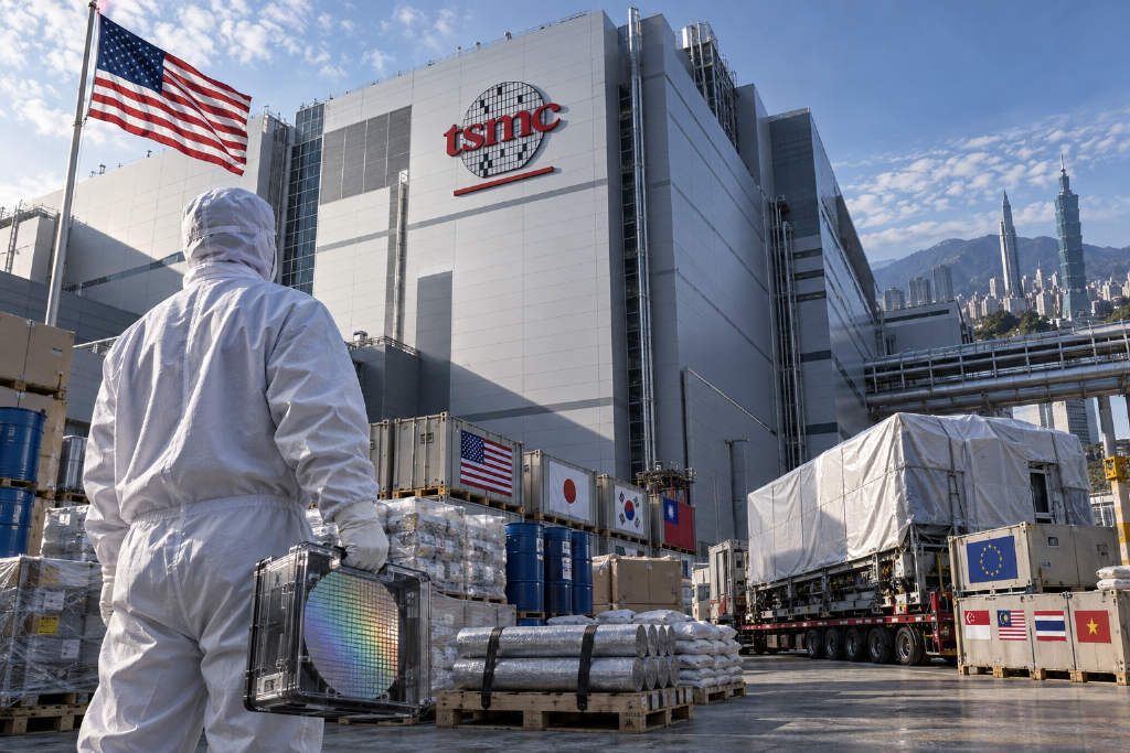
A new report from the U.S. Semiconductor Industry Association (SIA) says semiconductors are central to the country’s economy and national security, but the global upstream supply chain behind U.S. chip production contains fragile points that are often hard to see.

SIA said chips support applications ranging from smartphones and artificial intelligence (AI) infrastructure to medical devices, automobiles, manufacturing equipment and defense systems. For decades, tightly connected global supply chains helped U.S. chip companies lower costs while improving performance. Recent disruptions, the report said, exposed weak links in the upstream network supporting the U.S. semiconductor ecosystem and made the case for building a more trusted and reliable supply chain with less strategic dependence.
The report catalogs critical categories of materials and equipment used in U.S. semiconductor production, identifies weak points vulnerable to disruption, and lays out measures SIA believes are needed to strengthen the supply chain.
Three headline findings from the report
SIA grouped its conclusions into three broad findings.
- First, the semiconductor supply chain is multilayered and geographically dispersed. Chip production takes months and requires materials, equipment and components sourced from multilevel suppliers around the world. Of the roughly $27 billion in equipment and materials consumed by U.S. semiconductor companies, 95% comes from suppliers headquartered in the United States, Europe and Japan, but the actual manufacturing of those inputs is spread globally.
- Second, equipment and materials used for semiconductor production in the United States depend on fragile links buried deep upstream in the global supply chain. Many Tier 1 inputs rely on lower-tier raw materials and subsystem components that face elevated disruption risk, increasing exposure for the U.S. semiconductor ecosystem and partner countries.
- Third, protecting semiconductor supply chains requires a range of mitigation strategies. SIA said the U.S. government and industry need to work together and coordinate with like-minded global partners and allies.
What SIA says should be done
The report lays out several policy directions.
One is expanding domestic production and strategic reserves. SIA said moving all materials and equipment needed for semiconductor production back into the United States would be neither practical nor economical. For some critical inputs, though, building or expanding domestic capacity is a realistic and important near-term step. For others, new U.S. capacity could take 10 years or more to establish, followed by additional time to qualify materials for semiconductor manufacturing. The report said government and industry should work closely to identify and prioritize localization and reserve targets.
Another is building and maintaining ally-based supply chains. SIA said the supply chain supporting the U.S. semiconductor ecosystem is global by nature, and that strong trade relationships with allies and partner countries or regions, combined with investment in complementary supply chain capabilities, are essential for resilience.
A third is reducing reliance on unreliable sources of rare earths and critical minerals. According to the report, recent export restrictions on critical minerals and rare earth elements show the urgency of building new mining and processing capacity in the United States and partner economies. Coordinated policies such as long-term offtake agreements are also important to sustain demand for new capacity.

SIA also called for more research and development spending. Governments in the United States and partner countries or regions should increase and sustain funding for materials science, chemistry and engineering research tied to next-generation semiconductor materials and recycling processes.
The report says a trusted and dependable supply chain for the U.S. semiconductor ecosystem will require continuing coordination among government, industry and international partners. It argues that the findings can help lower the risk of future disruptions, reinforce key supply chain partnerships and strengthen U.S. chip leadership over the long run.
Why SIA says supply chain stress is becoming more visible
In the introduction, the report describes semiconductors as a foundational enabling technology for industries across the U.S. economy and for emerging technologies. Whether the product is an advanced logic chip, an analog or mixed-signal chip, a compound semiconductor device or a memory device, manufacturing usually takes months, involves repeated cross-border shipment, and depends on a highly specialized and carefully coordinated supply chain for materials and equipment. SIA said supply must arrive on time and in sufficient volume to meet industry demand, adding that global semiconductor sales are expected to exceed $1.5 trillion in 2026.
The report cites the U.S. Department of Commerce’s 2023 "Assessment of the U.S. Microelectronics Industrial Base," which said semiconductor manufacturing "requires hundreds of distinct materials with exacting quality requirements" and that maintaining a strong domestic manufacturing base depends on a materials supply chain able to withstand regional shocks or disruptions tied to individual companies.
SIA said global semiconductor supply chains have been disrupted in recent years by natural disasters, the Covid-19 pandemic, supply-demand imbalances and government actions. As companies invest in U.S.-based semiconductor manufacturing capacity, concern has grown that key upstream weaknesses could slow expansion plans and delay projects.
Some vulnerabilities, such as rare earth dependence, are already well known. Others may sit in upstream layers that appear lower risk until a disruption reveals them. To identify those deeper weaknesses, SIA worked with procurement, supply-chain and strategy leaders across the semiconductor ecosystem, including chip manufacturers, fabless chip design firms, back-end packaging companies, equipment makers and material suppliers.
The effort was designed to answer three questions: which upstream inputs create severe vulnerability for the U.S. semiconductor ecosystem, which materials and equipment used in chipmaking are themselves exposed through fragile upstream chains, and what steps government and industry stakeholders can take to reduce those vulnerabilities and build a more resilient supply base.
How the report measures vulnerability
SIA defines supply-chain dependence as the suppliers, materials, equipment and services semiconductor companies rely on to support design and manufacturing. It defines vulnerability as a weak point in that network that faces a higher risk of supply disruption, malicious exploitation or policy shock. Not every dependence is a vulnerability, the report says, and not every vulnerability is high risk.
To assess which dependencies create serious risk for the U.S. semiconductor ecosystem, SIA built a systematic and quantifiable vulnerability index. The index combines five factors: geographic concentration of production, degree of dependence, supplier concentration for specific products, ownership structure of critical suppliers, and dependence at lower supplier tiers. Each input was scored across the five factors and then rolled into a composite index.
Headquarters data and production-location data tell different stories
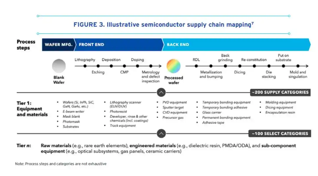
The report divides semiconductor manufacturing into front-end processes carried out on wafer surfaces and back-end processes that package dies into finished chips. Manufacturers work with more than 1,000 Tier 1 suppliers to directly purchase raw wafers, specialty gases, photoresist chemicals and other materials, along with production tools such as lithography systems and deposition equipment. Those Tier 1 suppliers also rely on complex sub-tier networks of intermediate products and raw-material providers.
For the analysis, SIA assembled one list of 200 critical Tier 1 equipment and material inputs covering both front-end and back-end semiconductor operations, and another list of 100 categories of raw materials, engineered materials and subcomponents or equipment in lower tiers. It then mapped these supply chains in detail, looking not just at where suppliers are headquartered but where inputs are actually produced.
SIA said supply-chain mapping in semiconductors often relies on supplier headquarters, which can mask real dependencies. Adding actual production location analysis is important for surfacing hidden dependencies and showing which ones may create severe vulnerability. The report said collecting this data required extensive research and validation with industry experts familiar with manufacturing processes and procurement patterns.
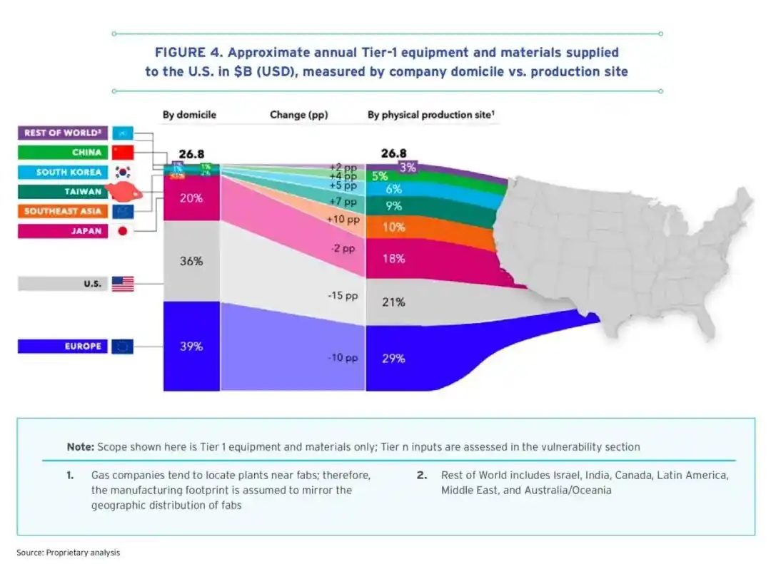
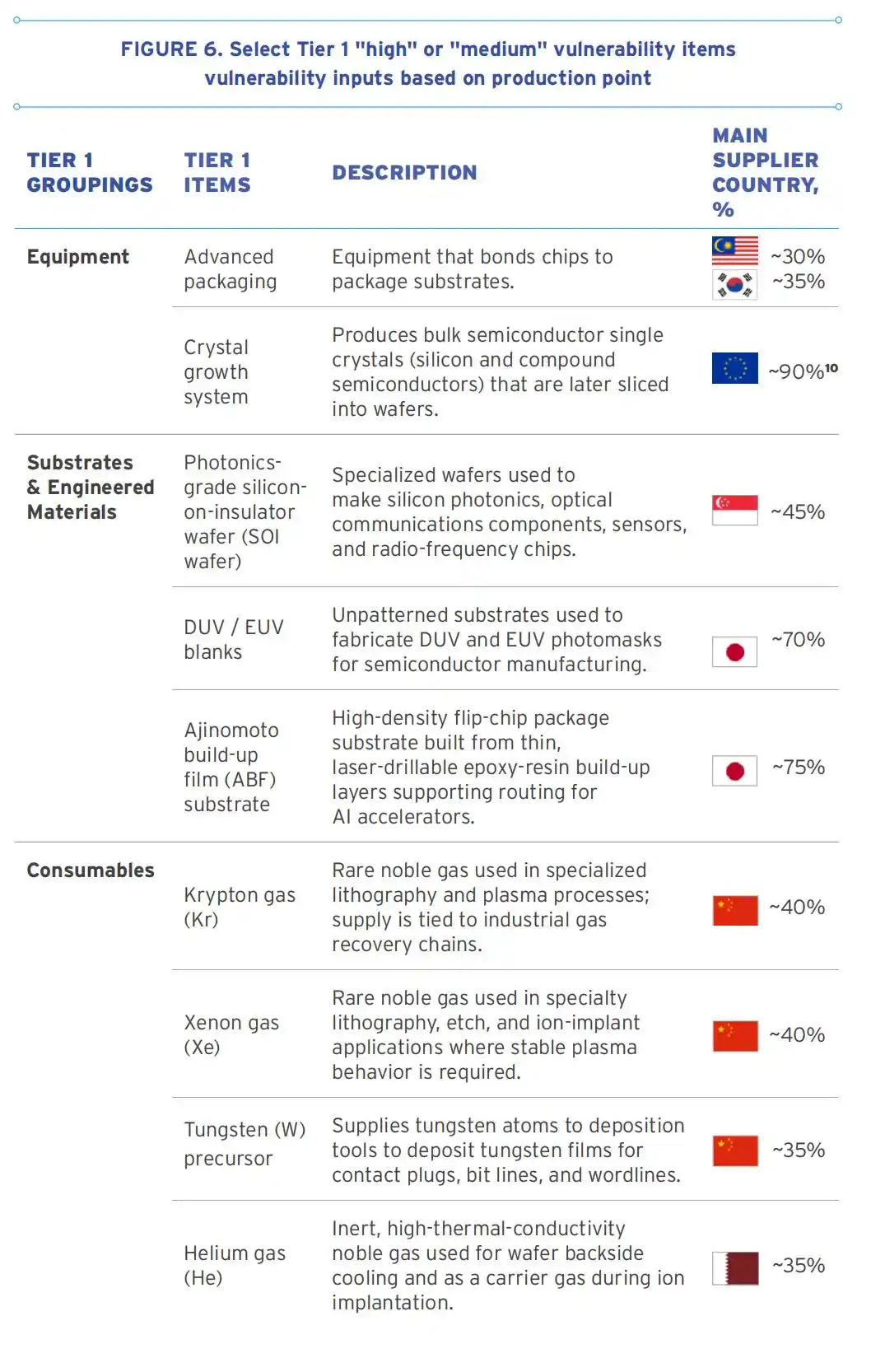
Based on Tier 1 analysis, the U.S. semiconductor ecosystem spends about $27 billion a year on equipment and materials, with 95% of supply coming from companies headquartered in the United States, Europe or Japan. The remaining roughly 5% comes mainly from firms headquartered in South Korea, Taiwan, mainland China, Southeast Asia and Israel.
When the same picture is redrawn by production or assembly location, dependence on the United States, Europe and Japan falls from 95% of total demand to 68%. Reliance on mainland China, Israel, Southeast Asia, South Korea and Taiwan rises from 5% to 32%.
SIA gives several examples. U.S.-headquartered semiconductor equipment suppliers assemble physical vapor deposition (PVD) tools in Singapore and etch tools in the United Kingdom. U.S. material suppliers produce photoresists and ultra-high-purity gases for chipmakers in chemical plants in Japan, Taiwan and South Korea. By contrast, bulk gases such as hydrogen and argon are often produced by European firms, but generation frequently happens near U.S. semiconductor wafer fabs through air separation units.
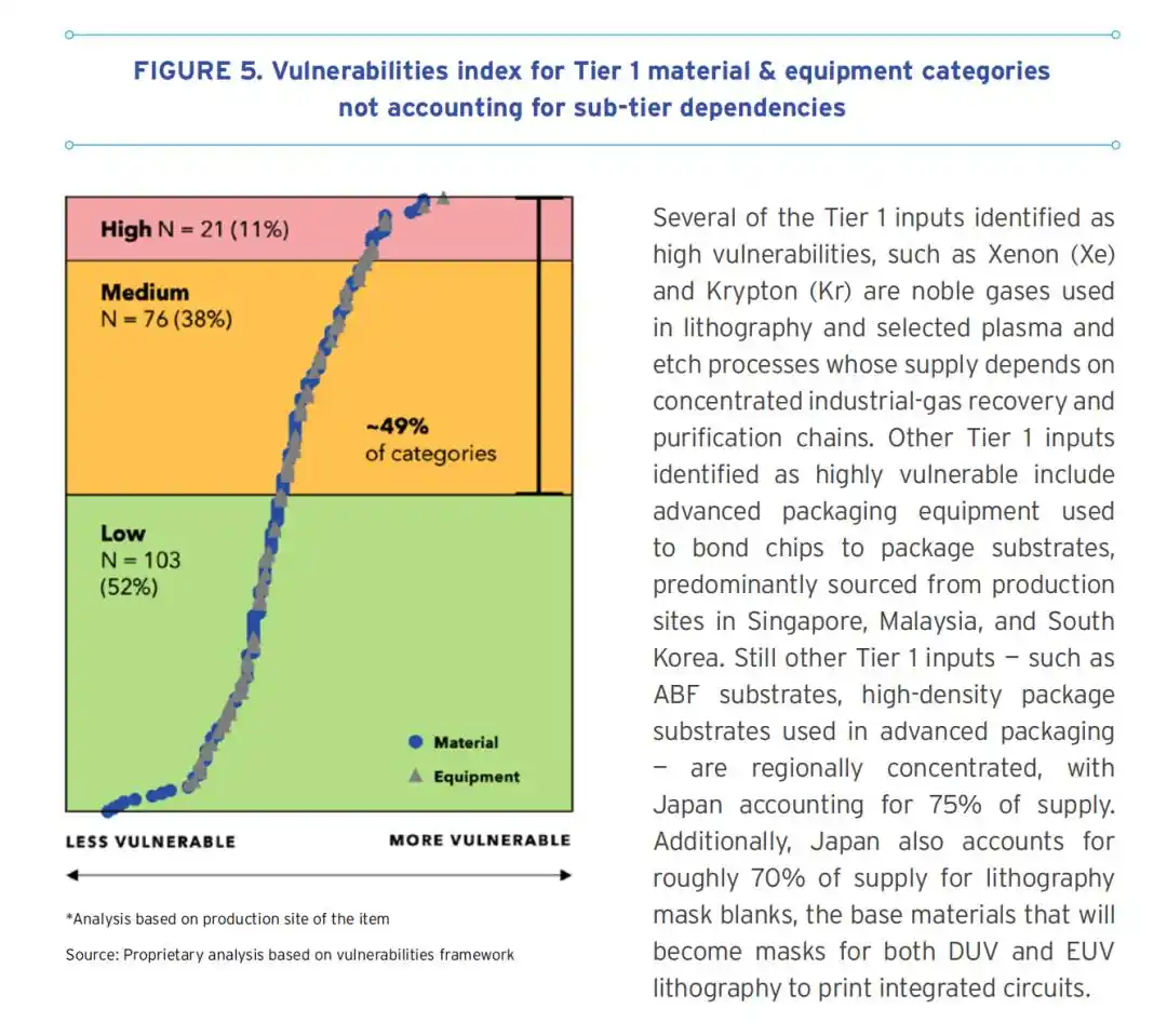
Using its vulnerability index on Tier 1 supply dependence, SIA found that about half of the categories analyzed fall into either high or medium vulnerability, with 11% rated high and 38% rated medium. The reasons vary by category: some are concentrated in a small number of production regions, some depend on a very limited pool of qualified suppliers, and some are exposed because of where production is located.
Upstream risks hidden below Tier 1
The report says semiconductor manufacturers and equipment makers usually do not buy raw materials directly from mining companies. They buy from specialized materials suppliers, which process minerals into high-precision chemicals, materials or components such as batteries and motors used in machine tools. That means firms supplying Tier 1 inputs for semiconductor production depend on deeper sub-tier networks made up of intermediate-product and raw-material suppliers. Those lower tiers can also be disrupted, affecting Tier 1 stability.
SIA points to measures taken by China to restrict the global supply of upstream critical materials including gallium, germanium, graphite, tungsten and rare earths. Those materials are important inputs for many Tier 1 semiconductor materials and equipment categories. The report says this kind of supply-chain leverage may extend beyond critical minerals into other materials, components and production equipment where China is seeking faster domestic substitution.
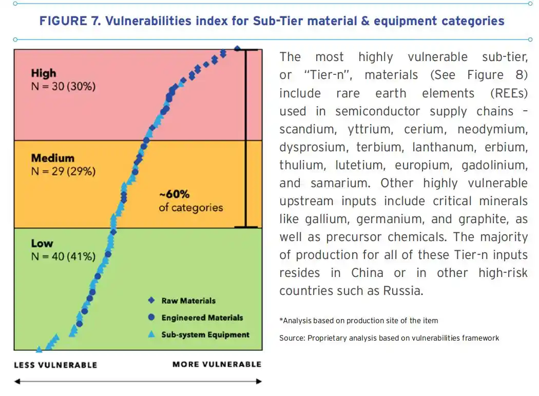
Because semiconductor supply chains are complex and multilayered, disruption risk accumulates as pressure travels upstream. To identify deep vulnerabilities that could be hidden inside the supply chains supporting the U.S. semiconductor industry, SIA mapped and analyzed nearly 100 selected upstream Tier-n inputs, including basic materials, engineered materials and subcomponents. It also assessed the vulnerability of those inputs.
Among the upstream inputs analyzed, nearly one-third were classified as high vulnerability.
China’s export controls on critical minerals are treated as a major factor
The report devotes a section to Chinese export controls on critical minerals. It says the Chinese government imposed export restrictions in 2023 on key semiconductor raw materials including gallium, germanium and graphite, and that these measures were upgraded to export bans the following year. In April 2025, China imposed export controls on seven medium and heavy rare earth elements used in magnet production and advanced manufacturing. In October that year, the scope was expanded to cover additional rare earth categories, mining and smelting equipment, and rare-earth-related technology.
SIA also cited Chinese customs data showing that, as of June 2026, Chinese exports to Japan of some controlled critical minerals, including gallium, dysprosium, terbium and yttrium, remained at zero or trace levels. Because Japanese suppliers play a major role in supplying the United States with semiconductor materials, components and manufacturing equipment, the report said prolonged restrictions on those raw materials could create additional downstream supply risk for the U.S. semiconductor industry.
Rare earth elements and critical minerals are used widely across supply-chain tiers. Neodymium, dysprosium, samarium and terbium are used in permanent magnets, which are critical for semiconductor production tools such as wafer-handling robots and sputtering equipment. Scandium metal is added to aluminum alloys for radio frequency (RF) and bulk acoustic wave (BAW) filters used in 5G, Wi‑Fi and other wireless technologies, and is also an important material for microelectromechanical systems (MEMS) actuators and sensors. Gallium and germanium serve as precursor alternatives to silicon substrates in power semiconductors and photonics, while graphite is used in thermal-zone components for crystal growth furnaces.
Polysilicon is listed as another vulnerable upstream input. By purity, polysilicon is mainly split into solar-grade and electronic-grade material. China is the world’s largest polysilicon producer, with more than 90% of total capacity, almost all of it solar-grade. Electronic-grade polysilicon used in semiconductors requires extremely high purity, at 99.999999999%. Although a small group of producers in the United States, Europe and Japan controls about 85% of the electronic-grade market, those suppliers still depend on large-scale solar-grade production to achieve the economies of scale and utilization needed for ultra-high-purity semiconductor-grade output.
The report says the rapid expansion of China’s solar-grade polysilicon capacity, combined with advances in electronic-grade process technology, is creating stronger competitive pressure and increasing risk for existing qualified suppliers.
SIA also says some Tier 1 materials and equipment rated low or medium on initial review carry hidden vulnerability because they depend on highly vulnerable Tier-n basic materials. Under the initial index, only 21 Tier 1 inputs were classified as high risk. Once sub-tier dependencies are included, more than three-quarters of the Tier 1 supply categories analyzed are linked to at least one extremely vulnerable Tier-n input, and more than half depend on two or more such inputs.
Domestic capacity and stockpiles: some options are long-term, some are immediate
In the section on mitigation strategies, SIA says categories rated medium or high vulnerability should be met with tailored resilience measures. It argues that while stronger domestic capacity is attractive, a single approach centered only on expanding U.S. production would be impractical, inefficient and in some cases impossible.
Depending on the category, it could take 10 years or more before U.S. domestic capacity delivers meaningful supply volumes. Even after new production begins, bringing upstream suppliers into semiconductor-grade supply chains and completing qualification for new materials often takes another three to four years.
Still, for some critical inputs, establishing or expanding U.S. capacity is considered a realistic near-term step. SIA says most Ajinomoto build-up film (ABF) substrates and photoresists come from Japan, and that investment in U.S. capacity to support domestic wafer and chip production would improve supply-chain resilience. The report also says that although advanced wafer capacity is expanding inside the United States, new capacity still falls short of domestic chipmaking demand. Sputtering targets, where the U.S. already has some manufacturing presence, are named as another area suited for domestic expansion.
SIA said the U.S. government should consider targeted incentives for equipment and materials companies to invest in domestic capacity for high-priority inputs. It also referred to an earlier SIA proposal in which federal and state governments, working with industry, would establish economic zones or technology parks to encourage suppliers to cluster near semiconductor manufacturing hubs.
For other key materials, subsystems and components, strategic stockpiles are presented as a way to bridge gaps while waiting for new suppliers to come online. The report says semiconductor manufacturers already use excess inventory to protect against disruption and, where possible, often hold as much as 12 months of supply. Examples include rare-earth magnets, neon, and motors and motor components. Tungsten sputtering targets used in physical vapor deposition are also described as suitable for stockpiling.
Not every input can be stockpiled, however, and shelf life is one reason. SIA notes that scandium metal is especially difficult to store because it oxidizes quickly and has a shelf life of only nine to 15 months.
In other cases, regulation limits stockpiling. SIA points to fluorinated gases used in semiconductor manufacturing, which are subject to U.S. and global environmental rules that make it difficult for companies to establish multi-year buffers. These gases are used in plasma processes, dry etching and chemical vapor deposition tool cleaning, and their raw material source is fluorite. More than 60% of global fluorite supply comes from mines in China. The report says the U.S. government could consider exemptions under current environmental rules to allow semiconductor manufacturers to import and stockpile such gases, including halocarbons. It also says Washington could work with allies such as Mexico, which has large fluorite mines, to increase output, and could use tax or other fiscal incentives to encourage reserves.
Allied supply chains remain central in SIA’s view
SIA says it is not practical, economic or feasible to bring all production of materials and equipment needed for U.S. semiconductor manufacturing back onshore. To support shared economic growth and security, the report says, the United States must work with partners and allies to diversify critical supply chains and collaborate on future technologies.
That means a key part of protecting vulnerable links is not only building domestic supply capacity but also maintaining strong relationships with allied and partner supplier countries and investing in their industrial capabilities. The report names Japan, Taiwan, Malaysia, Singapore, South Korea and several European partners, including Germany, France, Italy, the Netherlands and the United Kingdom, as important production locations for critical engineered materials and components used in semiconductor manufacturing equipment.
Those producers, in turn, rely on critical mineral feedstocks from other regions, including Australia, Canada, India and Mexico, all of which have mining and refining capacity for minerals needed in semiconductor production. The report also says cooperation with Vietnam and Indonesia, including public-private investment in local refining and processing infrastructure, could help expand capacity outside high-risk regions and support resilience.
Materials science, recycling and commercialization also feature in the recommendations
SIA says sustained government support for basic and applied research in materials science, chemistry and engineering can reduce upstream vulnerabilities by developing new technologies and finding what the report describes as inventive breakthroughs for existing challenges.
It cites two examples. One is the Minerals to Materials Supply Chain Facility, or METALLIC, funded by the U.S. Department of Energy and involving nine U.S. national laboratories, which the report says could open new extraction and processing pathways for mineral production. The other is advanced materials research grants offered by the Department of Commerce’s CHIPS Program Office.
Funding for recycling research is also highlighted as a way to recover useful materials from electronic waste and other discarded electronics. The report says emerging wafer recycling technologies for silicon carbide (SiC) substrates can cut substrate consumption per device by as much as 10 times. More research into storage methods that extend shelf life could also improve buffer-stock capability for critical materials.
SIA says support should come in several forms: public funding for national laboratories and universities working on new materials, process technologies and metrology, and assistance for private companies scaling electronic-waste recycling to recover critical minerals and materials. As new technologies emerge, the report says government also has a key role in creating policy frameworks that support technology transfer and licensing from upstream research programs to commercial firms.
The report notes that the National Science Foundation, the War Department, now the Department of Defense, and the Department of Energy have long supported basic and applied research in semiconductors, materials science and related microelectronics science and engineering. Continued funding for research institutions, it says, is important if next-generation semiconductor materials and recycling technologies are to be developed and commercialized in the United States.
Rare earths and critical minerals are treated as a priority area
The report says the federal government should give special attention to the heavy dependence of U.S. and allied suppliers on rare earth elements and other critical minerals affected by export controls. New mining and processing capacity is urgently needed to supply the critical minerals used widely in semiconductor manufacturing.
Beyond increasing domestic mining and refining where practical, SIA says addressing these vulnerabilities will require coordinated work between the U.S. government and other governments to support raw-material extraction and processing projects already underway in Australia, Canada, Japan, Mexico and South Korea. These efforts include refining and separation partnerships, conversion and recovery from oxides to metals, and qualification work.
Coordinated policies such as long-term offtake agreements are important, the report says, to make sure demand is sufficient to support new critical-mineral capacity. It also points to several multilateral initiatives, including the U.S. State Department-led Pax Silica initiative, the U.S.-EU Action Plan on Critical Minerals Supply Chain Resilience, and G7 leaders’ declaration on securing critical mineral supply chains.
Bottom line of the report
In its conclusion, SIA says the study shows both the complexity of the upstream supply chain that underpins the U.S. semiconductor industrial base and the hidden vulnerabilities that could obstruct efforts to build resilience if they are left unaddressed. Because semiconductors carry strategic importance for the U.S. economy and national security, strengthening the resilience of the global supply chain behind the domestic chip ecosystem is presented as a top priority for both industry and policymakers.
SIA says any comprehensive strategy needs a long time horizon and measures tailored to the characteristics and constraints of different supply segments. Since the supply chain supporting U.S. semiconductor companies is global, the report says the United States must also work with like-minded governments to build trusted and resilient supply chains. If those efforts continue, SIA says the U.S. semiconductor ecosystem and its broad customer base could become stronger, more resilient and more competitive over the next decade.
The article was sourced from the WeChat public account "Semiconductor Industry Watch" (ID: icbank), with SIA listed as the author.