
SK hynix has started building out a commercialization plan for 3D stacked DRAM-on-Logic technology aimed at next-generation memory for on-device AI. The company is recruiting design engineers through its U.S. subsidiary in California, and it has already begun joint development work with a specific North American customer. Analyst Jukan named Apple as the most likely counterpart.

As the industry shifts from generative AI toward physical AI, the report says 3D stacked DRAM is increasingly seen as a prerequisite for bringing on-device AI into practical use. But mass commercial adoption is still some distance away, both technically and commercially.
Why 3D stacked DRAM is being pitched as an answer to PoP limits
Most smartphones today use PoP, or Package-on-Package, for memory packaging. In that setup, two chips are stacked directly on top of each other. That approach worked when AI workloads on devices were relatively limited. For on-device AI, though, the constraints are becoming harder to ignore: longer chip-to-chip distance and a limited number of I/O channels create bandwidth bottlenecks and higher power consumption, making it difficult to deliver both high bandwidth and low power use at the same time.
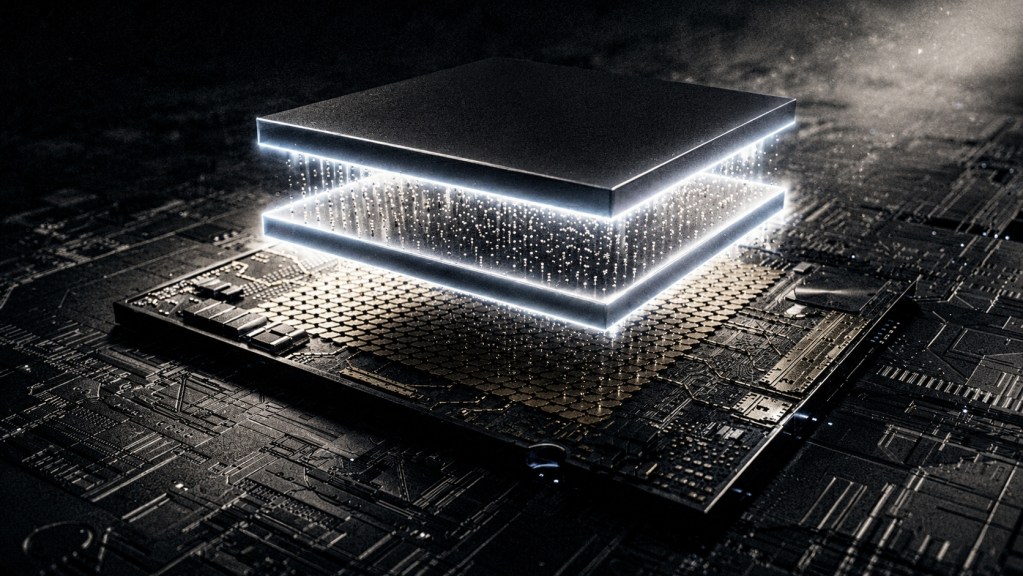
3D stacked DRAM-on-Logic is designed to tackle that problem at the architecture level. The technology vertically stacks DRAM directly on top of a logic die, sharply reducing the physical distance between the two while also increasing the number of data paths available within the same package footprint.
In the structure described in the article, the logic layer sits at the bottom and handles control and coordination, while stacked DRAM layers above it store data. TSVs, or through-silicon vias, run vertically through the stack and provide the conductive channels that make high-speed transfer possible.
Compared with PoP, the architecture can reduce transfer latency, improve power efficiency, and make better use of space. Those three points line up with what mobile AI inference needs most. The report adds that mobile application processors are viewed as the most promising early use case, with Apple and Qualcomm identified as the two leading players in that segment.
SK hynix splits its next-generation memory roadmap across three tracks
Ahn Hyun, head of development at SK hynix, said at the TSMC Technology Symposium in April that the company’s future differentiation strategy would cover three technology lines: customized HBM, HBF, or high-bandwidth flash, and 3D stacked DRAM-on-Logic.
In the article’s framing, these are not competing substitutes. They are meant for different environments. HBF targets the high-capacity needs of cloud AI inference by vertically stacking NAND flash and filling the memory-tier gap between HBM and conventional SSDs. The stated goal is to address the capacity pressure created by expanding KV cache requirements during large language model inference.
3D stacked DRAM-on-Logic, by contrast, is aimed at the low-power, high-bandwidth demands of edge AI and would be integrated directly with the core logic chips used in mobile devices. One track is built for capacity in cloud servers. The other is built for performance and power efficiency in end devices.
North American customer not disclosed, but Apple was singled out
Korean media outlet Zdnet, as cited in the source article, reported that a job posting from SK hynix’s U.S. subsidiary said the company was seeking engineers who could “closely collaborate with U.S. customers and lead co-design of 3D stacked DRAM logic chips,” with the aim of delivering “chip design solutions that meet evolving technology and market needs.”
As for the identity of that undisclosed North American customer, Citrini analyst Jukan said Apple was the most likely candidate. His reasoning was direct: “Apple has long developed its A-series and M-series chips in-house, places high value on performance gains from packaging integration, and has had long-term ties with SK hynix on memory technology.”
If that partnership proves to be real, the article says it would mark a major generational shift in Apple’s mobile AP memory architecture.
On-device AI still faces a long road to scale
Even so, Jukan argued that the underlying memory technology still has to catch up before on-device AI can move into broad deployment. He said, “3D stacked DRAM technology has to be in place first before on-device AI can truly scale, and that road is still quite long.”
He also added: “Unless vendors plan to cram 128GB of LPDDR into a smartphone, the current memory architecture simply cannot support the compute scale that edge AI really needs.”
As AI models keep expanding their context lengths, demand for memory capacity and bandwidth is rising quickly. At the same time, mobile devices have very little room to compromise on package size or power budgets. That is why 3D stacked DRAM-on-Logic is being treated as a possible route out of the current impasse.
Still, the path from hiring engineers to maturing the technology, then moving into mass production and end-product adoption, will take time and resources across the supply chain. Based on what has been disclosed so far, large-scale commercialization remains a longer-term prospect.