
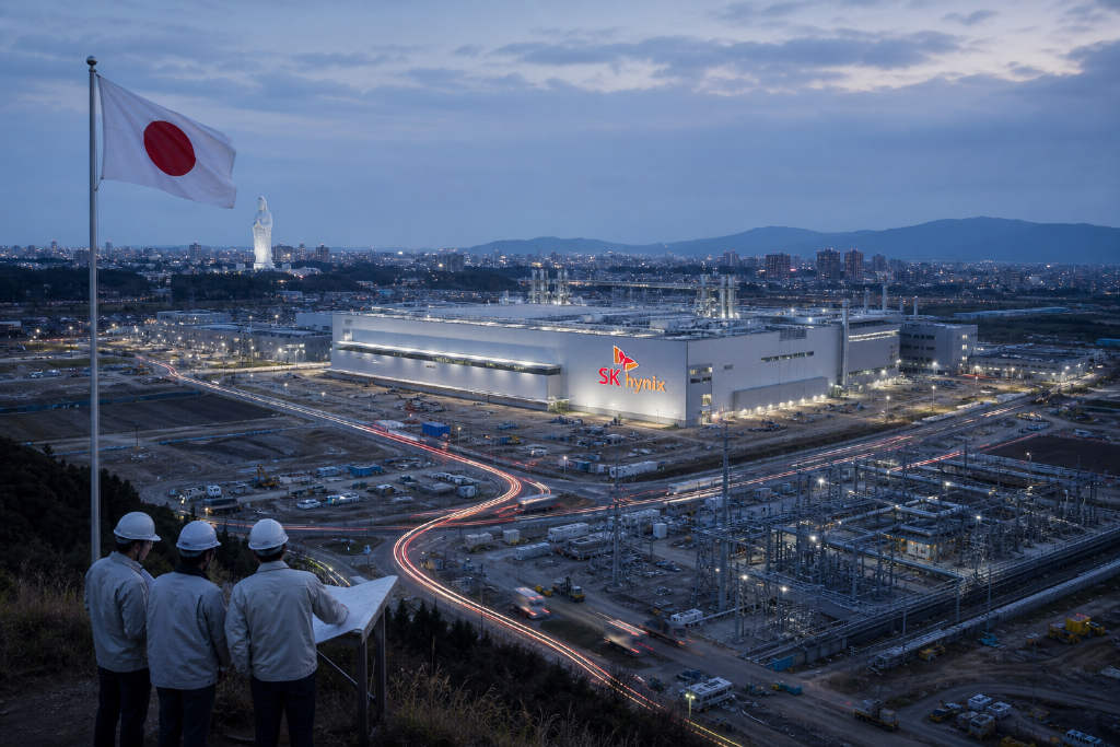
SK Group Chairman Chey Tae-won said in an interview in Sendai that SK Hynix is evaluating a plan to establish a memory joint venture in Japan, though he did not name a location or partner.
Korean media have reported that SK Hynix is pushing a proposal to invest tens of trillions of won in a memory wafer fabrication plant in Miyagi Prefecture. If the project goes ahead, it would make SK Hynix the third foreign company to build a large new fab in Japan after TSMC and Micron.
Miyagi offered land near Sendai
According to the report, Miyagi Prefecture has presented SK Hynix with a land proposal covering about 300,000 square meters near Sendai and is preparing water and electricity infrastructure. The goal is to reproduce the local economic effect Kumamoto achieved after bringing in TSMC.
SK Hynix is already planning a 54 trillion won capacity expansion in South Korea, equal to about $39 billion, and is also building an advanced memory packaging plant in Indiana.
Company says nothing has been decided
After a request for clarification from the Korea Exchange, SK Hynix said in an Aug. 21 filing that it is reviewing several measures, including the addition of new production sites, to strengthen the competitiveness of its memory business. The company said there are no final decisions at this stage and that it will provide another disclosure once specific details are confirmed or within one month.
This is not the first time a possible Japan facility has surfaced. Nikkei reported on the possibility in February, and Chey said in a June interview with Nikkei that Japan, with its power and materials ecosystem, is 「a very good candidate」.
HBM and NAND demand is driving the review
The overseas expansion review comes as memory supply remains tight. Demand has risen not only for high-bandwidth memory, or HBM, but also for NAND flash. The report said companies making large investments, including Meta and Amazon, are competing to secure high-capacity storage that is faster than traditional hard drives.
SK Hynix also indirectly holds a significant stake in Tokyo-based Kioxia. Japan hosts a large concentration of supply-chain partners, and a local plant could help the company deepen ties with customers and suppliers there, in addition to cost considerations.
Japan investment could add to U.S. pressure
U.S. Commerce Secretary Howard Lutnick publicly called in July for SK Hynix and Samsung to build front-end wafer fabs in the United States. SK Hynix's Indiana project is a back-end packaging plant. If the company confirms a wafer fab investment in Japan, pressure from Washington to build in the U.S. could intensify.
Japan has a record of offering large subsidies to foreign chipmakers expanding production, with TSMC's Kumamoto plant serving as a leading example. Micron already operates a plant in Hiroshima, while Samsung Electronics has only established a next-generation packaging R&D base in Yokohama.