
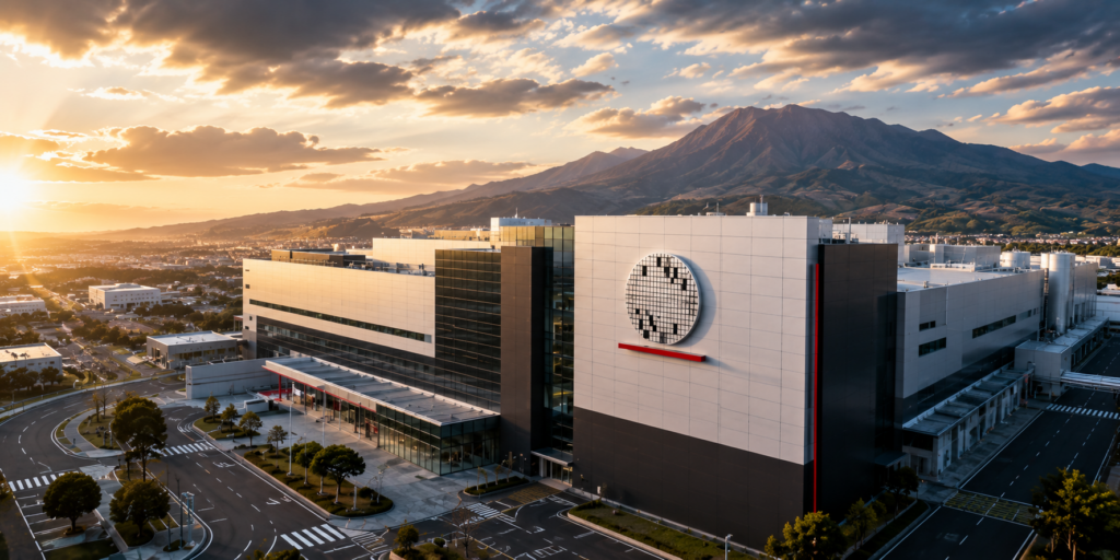
A 7.1-magnitude earthquake that struck Kumamoto on July 28 briefly brought production at Japan Advanced Semiconductor Manufacturing, or JASM, to a full stop and reignited scrutiny of Taiwan Semiconductor Manufacturing Co.’s choice of location. The plant has since resumed operations gradually over several days. According to the source article, the case for Kumamoto rests on a cost calculation that combines Kyushu’s long-built chip cluster, local supply chains, customer proximity and Japanese state subsidies.
The quake disrupted JASM and other Kyushu chip plants
The earthquake hit on July 28 and, according to the article, was the strongest tremor recorded in the area since the 2016 Kumamoto earthquake nearly a decade ago. JASM registered a seismic intensity of upper 5 at the site. Employees were evacuated, production was halted across the plant, and construction at the second fab was temporarily suspended. Sony, Renesas and other semiconductor facilities in Kyushu also paused operations briefly for inspections.
That quickly pushed one question back into view: was building a wafer fab in a seismic zone a strategic mistake?
Kyushu already has a decades-old semiconductor base
The article’s main argument is that Kumamoto is not an isolated greenfield decision. Kyushu began building semiconductor plants in the late 1960s and was known as Japan’s “Silicon Island” by the 1980s. At one point, IC output from the region accounted for about 40% of Japan’s total.
By 2016, Kyushu had gathered 40 semiconductor companies, 31 electronics companies and 39 equipment companies, the article said. It names SUMCO as a wafer supplier, Tokyo Electron as an equipment supplier, Tanaka Denshi Kogyo as a packaging-materials supplier and Advantest as a testing provider. Mitsubishi Electric and Renesas Electronics also operate nearby power semiconductor and automotive chip lines.
The local resource base matters too. Groundwater from the Aso mountain system is described as a lifeline-grade input for wafer fabs, while electricity costs are relatively low. Recreating that package in another prefecture or another country would require starting over.
Customers are next door
The customer map is just as important. JASM’s site sits next to Sony’s key image sensor plant, and CMOS image sensors require large volumes of mature-node logic chips. Demand tied to Denso and Toyota’s automotive operations has also already formed a full industrial cluster in Kyushu.
The article cites TSMC Chairman and CEO C.C. Wei as saying that the company builds where customer demand is. In Kumamoto, that line is presented almost literally on the map.
More than $20 billion in investment and about ¥1.2 trillion in subsidies
The financial side is substantial. The article says JASM’s two fabs carry more than $20 billion in combined equipment investment, with the second fab accounting for about $13.9 billion. Japan’s government support reaches a maximum of roughly ¥476 billion for the first fab and roughly ¥732 billion for the second, for a combined total of about ¥1.2 trillion. That means the public sector is covering around 40% of the investment.
Ownership is listed as about 86.5% for TSMC, 6.0% for Sony Semiconductor, 5.5% for Denso and 2.0% for Toyota. Combined monthly capacity at the two facilities is projected to reach 100,000 12-inch wafer equivalents.
The article also places the project in a geopolitical context. Japan is a G7 member and a U.S. ally in the Asia-Pacific region, which fits TSMC’s strategy of spreading advanced capacity across allied economies. In that sense, Kumamoto is not an investment that can be easily abandoned and rebuilt elsewhere.
The risk is real, and 2016 is the benchmark
The article does not dismiss the seismic threat. It recalls the 2016 Kumamoto earthquake sequence, with a 6.5 foreshock on April 14 and a 7.3 main shock on April 16, linked to activity along the Futagawa and Hinagu fault zones. Surface fault displacement stretched for about 30 kilometers.
At that time, Sony’s main image sensor plant in Kikuyo registered upper 6 on Japan’s seismic intensity scale. Precision equipment on higher floors was damaged, full process recovery took three and a half months, and losses reached ¥28 billion.
That history matters because it shows the fault risk is not hypothetical. The current quake also forced a work stoppage at JASM’s second fab under construction. At the same time, temporary inspection shutdowns at Sony, Renesas and other Kyushu plants suggest the earthquake is a common variable for the whole Silicon Island supply chain, not a TSMC-only problem.
Industry players stayed and kept expanding
The comparison the article emphasizes is Sony’s response after 2016. Despite taking ¥28 billion in losses, Sony did not leave Kumamoto. It continued to expand in the same Kikuyo area, and JASM was built beside Sony’s plant.
Under that logic, if seismic risk had truly become unacceptable, Sony would have been the first company expected to move, not TSMC, which entered the region a decade later. Sony’s decision to stay and add capacity is treated as evidence that recovery costs remained lower than relocation costs.
Earthquake engineering is about restart time and loss control
The article frames the issue this way: the point of seismic engineering is not to eliminate earthquakes, which cannot be controlled. It is to turn that uncertainty into variables a manufacturer can estimate, insure and book into financial planning — how long recovery takes and how much damage is done.
When JASM opened, TSMC said its overseas fabs use high-spec seismic design, including equipment anchoring, anti-seismic structures and emergency shutdown systems. The article argues that the latest 7.1-magnitude event, with the site registering intensity 5 and resuming production step by step within days while maintaining structural safety, served as a live test of that approach.
The article’s conclusion: recovery is cheaper than relocation
The source ultimately argues that Kumamoto remains a rational choice for TSMC as long as the expected loss from a single quake stays below the opportunity cost of giving up six decades of industrial clustering, the local supply chain and ¥1.2 trillion in subsidies.
It adds one condition. That calculation only holds if a direct fault rupture does not pass beneath the fab site itself.