
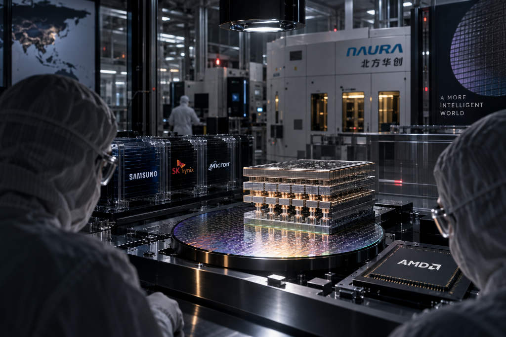
Two announcements in the first week of September 2026 jolted the memory chip sector. AMD said at an internal technical seminar that a 3D DRAM architecture built on Hybrid Bonding could deliver as much as 17x higher energy efficiency than a conventional high-bandwidth memory, or HBM, stack. At nearly the same time, NAURA published an IEEE paper saying it had made a major process breakthrough for next-generation 3D DRAM manufacturing.
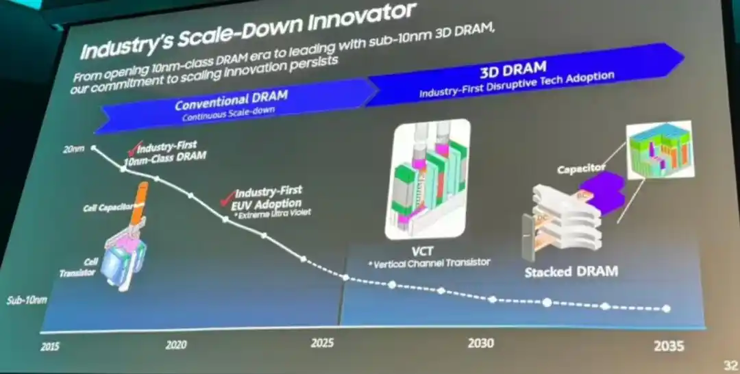
Taken together, the disclosures have pushed one question back to the front of the industry: why 3D DRAM is becoming a focal point for chipmakers and equipment suppliers worldwide.
AMD points to large efficiency gains from Hybrid Bonding
The number that drew the most attention from AMD was the claimed energy-efficiency gain. According to the company, its Hybrid Bonding-based 3D DRAM architecture can improve efficiency by up to 17x compared with a traditional HBM stack, implying a step change in data-transfer efficiency under the same power budget.
Conventional HBM already stacks DRAM dies vertically through through-silicon vias, or TSVs. Even so, the dies still rely on micro-bumps for interconnect. Those solder bumps create physical gaps that must be filled with liquid underfill material, which introduces parasitic resistance, limits interconnect density, and makes heat dissipation more difficult.
AMD’s approach overturns that design choice. It places DRAM dies directly on top of an XPU, meaning a processor or accelerator, removes the traditional PHY interface bottleneck, and replaces micro-bumps with direct copper-to-copper bonding. To make that possible, wafers are polished to atomic-level flatness before Cu-Cu bonding is completed under heat.
The benefit is not limited to interconnect efficiency. Putting DRAM directly above the compute die sharply shortens the physical path that data has to travel. In AI accelerators, where data movement consumes a large amount of energy, that distance reduction translates directly into lower power use.
NAURA details an etch process aimed at 64-layer structures
AMD’s disclosure was centered on architecture and bonding. NAURA’s paper focused on process technology. The company said it developed a new two-step cyclic etch process for a 64-layer structure built from alternating silicon and silicon-germanium, reaching structural uniformity above 95%.
The paper also disclosed several technical metrics: an etch selectivity above 500:1 between silicon-germanium and silicon, and silicon loss controlled to within 10 angstroms, or 1 nm, per cycle in a 200 nm interlayer structure.
The challenge is straightforward to describe and difficult to solve. In a stack with dozens of alternating layers, engineers need to remove one target layer precisely without damaging the neighboring layers. Under high-aspect-ratio conditions, lateral selective etching has long been one of the industry’s hardest problems. If selectivity is too low, the silicon framework is damaged. If byproducts accumulate at the bottom, etch non-uniformity between layers rises sharply and yields can fall just as fast.
NAURA’s method breaks the sequence into repeated etch and clean stages. In the first stage, unbiased neutral fluorine radicals are used to etch the silicon-germanium layer selectively while forming a dense germanium fluoride protective film on the silicon surface. In the second stage, reactive gases are introduced to clear bottom byproduct deposits so the etch chemistry can continue to penetrate vertically.
The article says that if a domestic DRAM manufacturer can integrate NAURA’s etch tools and related process know-how, the feasibility of moving toward independent mass production of 3D DRAM would improve substantially.
Why 3D DRAM is getting so much attention
The backdrop is the same across the industry: conventional DRAM scaling is moving closer to a ceiling. For years, DRAM followed a path similar to logic chips, relying on smaller process nodes to raise density. Once line widths approach below 10 nm, physical constraints become harder to ignore.
Unlike processors, DRAM stores data in capacitors. As the process node shrinks, capacitor dimensions become much harder to reduce further, while tighter transistor spacing raises short-circuit risk. On top of that, the high cost of extreme ultraviolet lithography, or EUV, tools and export controls have made the old path far less accessible for some players.
The basic idea behind 3D DRAM is to stop relying solely on planar scaling and move toward vertical stacking. Instead of squeezing memory cells into a tighter two-dimensional layout, the architecture extends upward in the z direction to increase storage density.
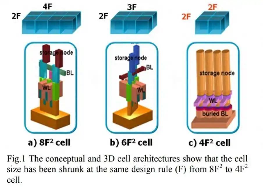
Two main routes are discussed in the article. One is 4F2 VCT DRAM, with VCT standing for Vertical Channel Transistor. The other is VS-CAT DRAM, short for Vertical Stacked-Cell Array Transistor. The first route centers on standing the cell structure upright. The second centers on multi-layer stacking in a form closer to 3D NAND and is often described as the more literal version of 3D DRAM.
DRAM cell size is usually compared with the design-rule unit F, or feature size. During the 2010s, the industry reduced cell area from the traditional 8F2 layout to 6F2 by improving array layout. With the same processing dimension, that cut cell area by 25%.
As the 6F² structure again approaches physical limits, 4F² is viewed as the theoretical density limit for a two-dimensional planar layout. The article says that, in theory, a 4F² architecture can integrate 30% to 50% more memory cells than a 6F² architecture in the same die area, which can be converted into higher capacity, faster throughput, and lower operating power.
Samsung, SK hynix, and Micron are following different versions of a similar playbook
The three largest memory makers are broadly taking a dual-track approach: they are working on 4F2 VCT-type structures while also developing VS-CAT, even if the naming and implementation details differ.
Samsung’s VCT approach places the transistor channel vertically, increasing channel length within a limited die footprint and easing the short-channel effects and leakage problems that come with planar scaling. On top of that, Samsung separates the memory-cell array and the peripheral circuitry onto different wafers, then stacks them vertically with inter-wafer copper hybrid bonding to achieve extremely dense interconnects. It has also shifted channel material from conventional silicon to indium gallium zinc oxide, or IGZO, to suppress leakage current in smaller cells.
According to Samsung’s roadmap cited in the article, the company plans to finish development of its 10a DRAM process this year, begin quality testing next year, and introduce the process into mass-production lines in 2028. Samsung is said to be applying its 4F² square-cell and VCT technologies across the 10a, 10b, and 10c generations. From the 10d node onward, it plans to move fully to a 3D stacked DRAM architecture.
At the more advanced 3D stage, Samsung is described as taking a more aggressive position. The article says Samsung Electronics has already achieved a 16-layer VS-CAT DRAM stack internally. Beyond raising capacity through stacking, VS-CAT DRAM is also expected to reduce current interference. Samsung expects to use a dual-wafer structure that separates memory cells from peripheral logic because a conventional single-wafer design would come with severe area penalties. After the memory-cell wafer and logic wafer are fabricated separately, the final VS-CAT DRAM product requires wafer-to-wafer, or W2W, hybrid bonding.
SK hynix is following a very similar strategic logic, though the naming differs. It calls its 4F² structure Vertical Gate, or VG, instead of Samsung’s VCT.
At the 2025 IEEE VLSI Symposium, SK hynix CTO Cha Seon Yong said the 4F² VG platform and 3D DRAM technology would be applied at 10 nm-class and below to overcome the scaling limits of existing platforms. The defining feature of VG is that the gate is placed vertically and wraps around the channel, making it fundamentally different from a traditional horizontal-gate structure.
SK hynix is also active on 3D stacking itself. The article says the company is accelerating development of 3D stacked DRAM, has started hiring related engineering talent, and is carrying out chip co-design work with U.S. customers. More recently, SK hynix said development of next-generation 3D DRAM semiconductors could use foundry processes. It is also exploring IGZO oxide semiconductors as the next channel material and using their low-temperature deposition characteristics to address thermal-budget constraints in 3D stacking.
Micron started earlier than many peers. The article says the U.S. memory maker began work on 3D DRAM in 2019. TechInsights data cited in the report shows that by August 2022, Micron held more than 30 3D DRAM patents, compared with 15 for Samsung Electronics and about 10 for SK hynix. On that count, Micron’s portfolio was roughly two to three times the size of those held by the two South Korean rivals. But the report says there has been little visible movement on mass production, and Micron has remained ambiguous about introducing a 4F2 memory cell.
Equipment priorities are shifting with the process roadmap
The article contrasts the AMD and NAURA developments because they appear to point to different implementation routes. AMD’s Hybrid Bonding-based 3D DRAM concept is described as a die-to-die stacking route between bare dies. NAURA’s process breakthrough, by contrast, may be more closely tied to monolithic vertical integration within a single wafer rather than D2D bonding and packaging between multiple dies.
The broader DRAM manufacturing roadmap helps explain why that distinction matters. Before EUV, DRAM mainly relied on 193 nm immersion deep ultraviolet lithography. Once the industry moved below 20 nm, a single DUV exposure could no longer print the fine patterns required, forcing manufacturers to use multiple exposure and etch steps to piece circuits together. That method could still push scaling into the 1x nm range, but at the cost of more steps, higher expense, and tougher yield control.
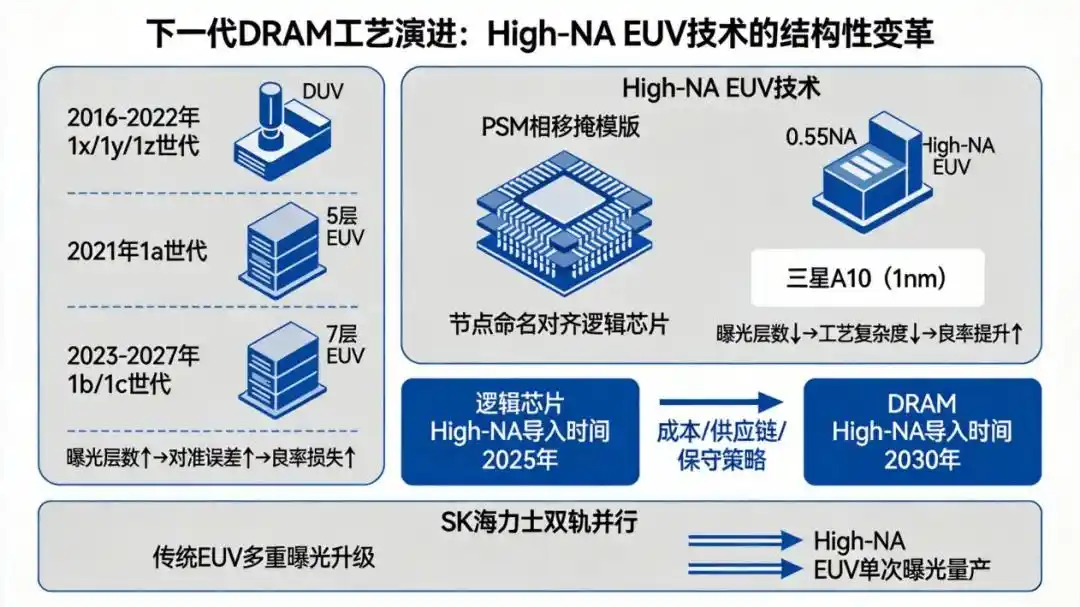
As the cost of multi-patterning approached its limit, EUV entered the picture. EUV has a wavelength of 13.5 nm and much higher resolution than DUV. In 2020, Samsung was first to ship 10 nm-class D1x DDR4 based on EUV, then fully introduced EUV at the D1a node. SK hynix and Micron followed afterward. The core reason for the transition was that EUV can reduce the number of multi-patterning steps, simplify process flow, improve throughput, and break through DUV’s resolution limit.
As DRAM keeps moving toward the 1δ node and beyond, conventional EUV is also nearing its limit, making High-NA EUV the next destination.
In August 2026, Samsung Electronics said at the NGL 2026 next-generation lithography conference that DRAM process nodes at A10, defined in the article as 1 nm, and below must adopt High-NA EUV, with production-line introduction planned for 2030.
At the same event, a vice president at SK hynix said the company had fully launched High-NA EUV research and development and was also introducing PSM phase-shift masks, described as mask materials that can control both light intensity and phase in order to suppress diffraction artifacts and unlock the theoretical resolution of High-NA EUV.
The article draws a clear conclusion from those roadmaps: the next phase of DRAM process evolution will move away from the last decade’s model of forcing scaling forward by adding more EUV exposure layers. In its place will come a stage where the number of exposure layers stops rising or even declines, node naming aligns more closely with logic chips, and mass-production timing is deliberately held back by two to three years.
Chinese suppliers are expanding beyond etch
The push into 3D DRAM in China is not limited to etch technology. The article says information from the website of the China National Intellectual Property Administration shows that a leading domestic 3D NAND company filed a patent in 2020 covering a DRAM design with the XTACKING architecture. XTACKING is the company’s proprietary architecture for 3D NAND and uses three-dimensional wafer hybrid bonding. According to the patent description cited in the report, the DRAM memory includes a first wafer with array transistors, a second wafer with capacitor structures, and a bonding interface between them that contains multiple bonding structures.
On the research side, a team led by Academician Liu Ming at the Institute of Microelectronics of the Chinese Academy of Sciences has studied the effect of the interlayer dielectric process before stacking a second device layer on the basis of a vertical annular channel IGZO FET structure. The work verified the reliability of CAA IGZO FETs in 2T0C DRAM applications and, according to the article, could help push the realization of a 4F² IGZO 2T0C-DRAM cell.
The equipment chain is shifting as well. After NAND moved into 3D, DRAM and advanced logic chips have been heading in the same direction, lifting demand for high-aspect-ratio etch, atomic layer deposition, and hybrid bonding at the same time.
The article says Advanced Micro-Fabrication Equipment Inc. China, or AMEC, introduced several newly developed high-end microfabrication tools during the 14th Semiconductor Equipment, Materials and Core Components Exhibition, CSEAC 2026. The products covered ultra-high-aspect-ratio etch, plasma-enhanced chemical vapor deposition, atomic layer deposition, metal film deposition, and silicon carbide epitaxy. It was the company’s second concentrated new-product showcase in six months, following the release of four products at SEMICON China in March.
Piotech is described as having natural technical synergies in hybrid bonding because of its strength in thin-film deposition. Its Dione 300 series wafer-to-wafer bonding tools can achieve high-precision bonding of multiple material surfaces at room temperature and are used in 3D ICs, advanced packaging, and CMOS image sensors, or CIS. The article also lists several other domestic suppliers by segment: Hwatsing Technology in CMP equipment, ACM Research Shanghai in cleaning tools for a leading domestic memory maker, Precision Measurement Electronics in optical inspection and metrology, Kingsemi in coating and developing tools, JIngce? No, the article separately names Jingzhida for memory-chip test equipment, and PNC Process Systems for high-purity process systems.
A bet on the future form of memory
From the dual-track roadmaps at Samsung and SK hynix, to Micron’s patent buildup, to NAURA’s progress in etch processes, the 3D DRAM contest is no longer confined to memory manufacturers. It is pulling upstream and downstream parts of the semiconductor supply chain into the same transition.
The original article frames the race as a wager on the future form of memory chips. The winner is still unclear. The direction, in its view, is not: after planar DRAM scaling approaches its limit, vertical architectures, stacking, and hybrid bonding are moving to the center of the next decade.
This article was sourced from the WeChat public account “半导体产业纵横” (ID: ICViews) and written by Feng Ning.