
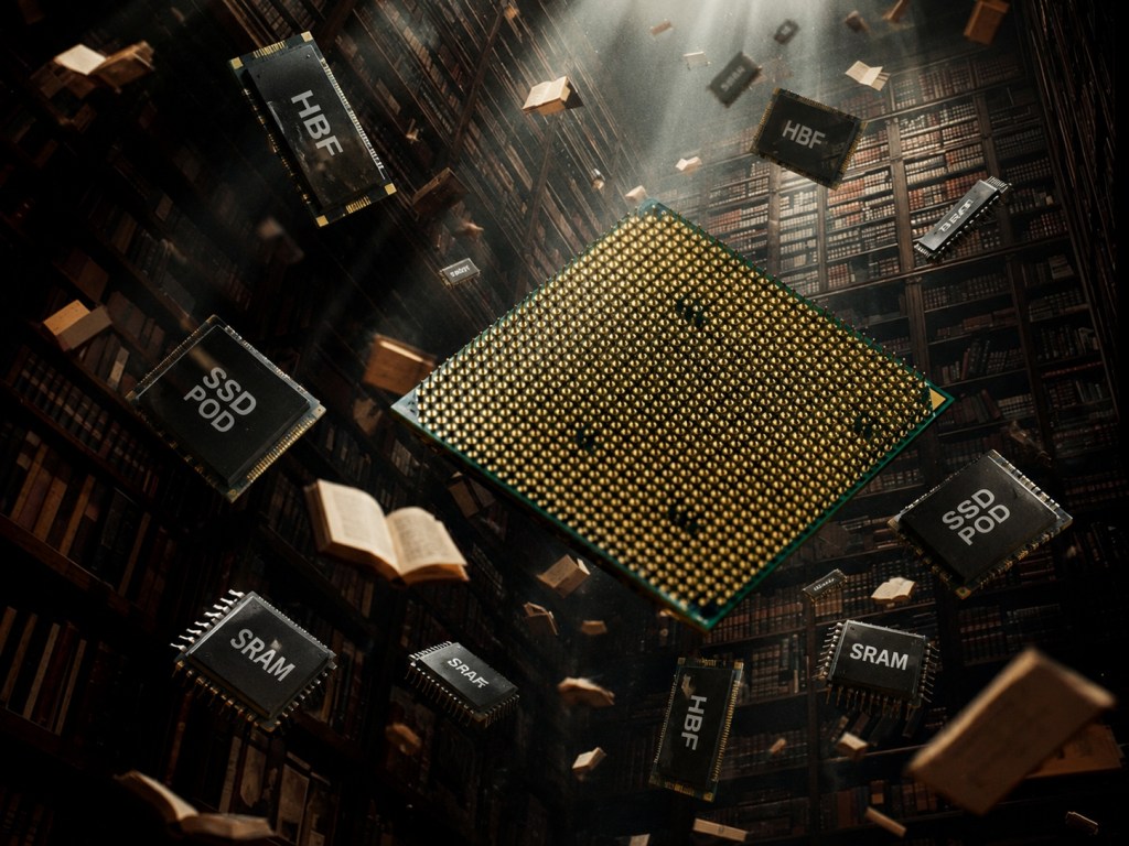
As AI spending shifts from training to inference, the memory hierarchy behind those systems is being reorganized as well. A new TrendForce research report frames the change around four technologies: HBM, HBF, SSD POD and SRAM. In the training era, HBM sat at the center because it addressed bandwidth. In inference, growing KV cache loads are turning capacity into a constraint alongside bandwidth, opening space for several new layers rather than one dominant standard.

The report’s core point is simple: HBF, SSD POD and SRAM are not competing to leave one winner. They are being positioned to handle different parts of an inference stack that is becoming more specialized.
Training and inference put very different demands on memory
AI training is the process of teaching a model new capabilities with large datasets. AI inference applies an already trained model to new inputs and generates responses. Those two stages access memory in different ways, which is one reason memory architectures have moved toward more specialized tiers instead of relying on a single dominant specification.
Using the Transformer architecture as an example, the training loop mainly consists of forward pass, backward pass and optimizer update. Because those steps repeat continuously until the model converges, memory access speed becomes a major driver of training efficiency.
Why HBM emerged in the training era
HBM, or High Bandwidth Memory, is built by vertically stacking multiple DRAM layers and linking them through TSV, or through-silicon via, technology. Instead of sending data over slower PCIe links, HBM is packaged alongside the compute die on the same interposer, cutting the data path sharply.
The report compares that setup with traditional DRAM connected over PCIe. PCIe 6.0 x16 delivers about 128 GB/s of one-way bandwidth, while a single HBM stack can provide more than 2 TB/s. HBM4 has already passed 1 GB/s of one-way bandwidth per pin, and one chip carries 2,048 pins. That jump in packaging and throughput is what allowed HBM to anchor the training era, creating a new memory layer between on-chip SRAM and conventional DRAM.
The report also describes the familiar rule inside training memory stacks: the higher the layer, the faster, smaller and more expensive it becomes; the lower the layer, the slower, larger and cheaper it gets. HBM earned its place by supplying the very high bandwidth training needed.

Inference changes the bottleneck with KV cache growth
Inference introduces a different pattern. The process is broadly divided into prefill and decode.
During prefill, the system processes the input prompt in parallel, computes and stores the key and value vectors for each layer, and produces the first output token. During decode, it reads those key and value vectors from KV cache, generates one token at a time, and keeps writing newly computed key and value vectors back into cache until the response is complete.
That decode loop is where the pressure builds. It repeatedly reads and writes KV cache on a per-token basis, and the cache itself expands with conversation turns, context length and batch size. At that point, HBM’s bandwidth edge alone is no longer enough to absorb inference demand. Capacity becomes a bottleneck too.
TrendForce argues that, compared with the relatively mature memory architecture used in training, inference memory design is still evolving quickly. Vendors are trying different approaches, and the hierarchy itself is in transition.
Three approaches taking shape over the next five years
The report lays out three routes now being used to address inference memory needs: HBF, SSD POD and SRAM.
HBF aims for much larger capacity with stacked NAND
To deal with the capacity growth of KV cache, SanDisk and SK hynix announced a partnership in August 2025 to develop HBF, or High Bandwidth Flash. In February 2026, they moved that effort into the Open Compute Project and created a dedicated working group to start global standardization. SK hynix has explicitly described HBF as a new memory layer between HBM and SSD.
Technically, HBF also uses vertical stacking, but it stacks NAND flash rather than DRAM and connects the layers with TSV. The report says the expected bandwidth is 1.6 TB/s, while a single HBF stack could provide about 512 GB of capacity. That is more than 10 times the capacity of HBM. For comparison, a 16-layer HBM4 stack holds about 48 GB.

The idea is to fill the gap between HBM and traditional DRAM. HBF has not entered mass production, though, and the report says market demand is not expected to fully appear until around 2030.
SSD POD extends cache into lower-cost storage tiers
Before HBF reaches production, many companies have already adopted KV cache offloading. The method moves less frequently used KV cache into lower memory tiers to ease the storage burden at the top of the stack. NVIDIA’s SSD POD concept is presented as a way to fill the gap between local SSD and shared storage.
The article points to NVIDIA’s explanation of its Dynamo framework. With the low-latency transport library NIXL, Dynamo can offload KV cache from limited GPU memory into CPU RAM, local SSD or remote network storage in real time without interrupting inference.
Storage vendor testing cited in the report shows a single H100 GPU reaching 35 GB/s of throughput. In a system built with eight H100 GPUs, read throughput can reach as high as 270 GB/s. That, the report says, suggests storage is no longer the limiting factor it once was for inference performance. It also helps explain why large-capacity, cross-rack storage architectures such as SSD POD are becoming more important.
SRAM pushes decode speed by keeping memory on chip
Another path has been taken by some inference-focused AI ASIC startups: put large amounts of SRAM directly on chip to get around HBM’s speed limits. The report names Groq and Cerebras as two examples. It also says NVIDIA acquired Groq’s inference technology licensing and core team in December 2025.
SRAM is faster than HBM, which is fundamentally a form of DRAM, for two reasons given in the article. First, SRAM read access itself is quicker, at around 1 nanosecond, versus about 10 to 15 nanoseconds for DRAM. Second, SRAM sits on the same die as the compute cores, so data travels a shorter distance than it does with off-chip HBM.
That speed comes with a capacity trade-off. Based on analysis from Gimlet Labs, a single Groq LPU chip carries only about 230 MB of SRAM. Supporting a 70 billion parameter model would require hundreds of chips linked together. Cerebras takes a wafer-scale approach instead, allowing a single chip to hold about 44 GB of SRAM and therefore support larger models with fewer chips.
The report says this is why SRAM is especially well matched to decode workloads, where token-by-token generation puts much heavier pressure on memory bandwidth than on compute density.
Product roadmaps are already shifting toward inference
The report ties the memory shift to recent hardware moves across the sector. NVIDIA has said it will bring Groq LPX chips into its Rubin product line, with shipments expected in the second half of 2026. It also introduced CMX, short for Context Memory Storage Platform, and the Vera CPU Rack.
Google has launched the TPU v8i for inference. Compared with the training-focused TPU v8t, the TPU v8i adds 72 GB of HBM3e and 384 MB of SRAM.
Inference-focused AI ASIC startups were active through the first half of 2026 as well. SambaNova launched its fifth-generation SN50 chip in February. Cerebras filed for an IPO in April and announced partnerships with OpenAI and Amazon Web Services. Etched said in June that its Sohu chip had successfully taped out at TSMC.
These technologies are being layered, not replaced
The article closes by distinguishing several points that often get blurred together.
- HBF versus HBM: HBM stacks DRAM and is built for bandwidth. HBF stacks NAND flash and is built for capacity, sitting between HBM and a traditional SSD tier to handle large KV cache loads.
- Will HBF replace HBM? No. HBF is meant to cover HBM’s capacity shortfall, not take over its bandwidth role. The report expects both to coexist in the same systems.
- Will SRAM replace DRAM? No. SRAM offers speed but is limited by chip area and therefore capacity. DRAM, including HBM, has density and cost advantages. The direction described here is layered deployment by workload, not full replacement.
- Is KV cache the same thing as SRAM? No. Traditional CPU and GPU cache memory is built with SRAM, but KV cache in AI inference refers to key and value vector data that is read and written frequently. It is a data structure, not the hardware medium itself.
TrendForce’s view is that the era of HBM as the single defining memory answer belongs more to training than inference. In inference, the stack is getting broader. HBF, SSD POD and SRAM are being assigned different jobs inside a more segmented architecture.