
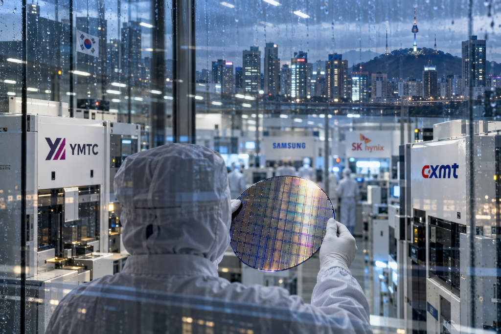
The technology gap between Chinese memory chip suppliers and the industry’s leading manufacturers is shrinking quickly, according to the latest assessment from the Korea Semiconductor Industry Association. The group’s view, as cited in a report, puts Yangtze Memory Technologies Co. (YMTC) about one year behind in NAND flash, while ChangXin Memory Technologies (CXMT) trails by roughly two years in DRAM and about three years in high-bandwidth memory, or HBM. Not long ago, that gap was widely seen as around five years.
JoongAng Ilbo cited the Korean industry association as saying: “The technology gap between Korea and China in memory semiconductors has narrowed to three years in HBM, two years in DRAM, and one year in NAND flash.”
NAND: YMTC could narrow the gap to about one year
According to the report, Samsung Electronics and SK hynix began producing 300-layer NAND flash in 2025, while YMTC was making 270-layer NAND at the time. By 2027, YMTC is expected to shift to 400-layer NAND, which could reduce its lag behind Samsung and SK hynix to about one year.
DRAM: CXMT is about two years behind in DDR5 timing
In DRAM, Samsung and SK hynix started producing DDR5 memory in 2023. CXMT began making DDR5 memory modules in 2025, leaving a gap of about two years.
The report also says CXMT has already entered mass production of LPDDR5X and has just started producing LPDDR6.
HBM: CXMT is still working through TSV challenges, with yields around 25%
In HBM, CXMT is currently about three years behind, the report says. It has just started trial production of HBM3E modules, but yields are only around 25%. The DRAM maker is still trying to master through-silicon via, or TSV, technology used for vertically connecting stacked memory.
The report says that in building HBM3E stacks on its G4 process, CXMT drew on ideas from YMTC’s X-Stacking 3D NAND approach. Instead of relying entirely on conventional micro-bumps to connect stacked DRAM dies, the design uses copper-to-copper hybrid bonding to merge copper interconnects between wafers and shorten circuit paths between stacked DRAM layers.
A key point in the report is that this architecture could allow CXMT and YMTC to produce competitive HBM designs without depending on extreme ultraviolet, or EUV, lithography tools.
The article also says CXMT is expected to receive some domestically made DUV lithography equipment this year from suppliers including Shanghai Aisijiena and Yuliangsheng (phonetic transliteration). At the same time, those DUV equipment manufacturers still face bottlenecks, especially in projection lenses and light sources.
Capacity expansion: CXMT targets 300,000 DRAM wafers per month by the end of 2026
CXMT is pushing an aggressive expansion plan. The report says the company aims to reach monthly capacity of 300,000 wafers by the end of 2026 through three 300 mm DRAM fabs, with each fab designed for about 100,000 wafers per month.
Its HBM wafer capacity is also expected to reach about 50,000 wafers per month by the end of 2026. CXMT is now building two new fabs in Shanghai and Hefei. Once those facilities come online, monthly capacity is expected to rise to 600,000 wafers.
The report adds that CXMT could surpass Micron in mass-production scale before 2030.
Technology roadmap: HKMG, 1z, and next-generation 15 nm G5
To deal with scaling limits, the report says CXMT is using high-k metal gate, or HKMG, technology. The process replaces older silicon-based insulators with materials such as hafnium oxide (HfO2), which can reduce current leakage and related heat loss, improve power efficiency, and support faster switching speeds.
Because CXMT has already applied the technology to its G4 DRAM manufacturing process and LPDDR5X products, the report says it is reasonable to infer that the company is moving toward the more advanced 1a node. It also says G4 is widely believed to use the 1z node, and that CXMT is already developing its next-generation 15 nm G5 DRAM process.
YMTC capacity outlook
For YMTC, the report says monthly capacity is expected to reach 300,000 wafers by early 2027, with part of that output allocated to LPDDR production. After two new fabs start operations in 2027, total capacity is expected to increase to 450,000 to 500,000 wafers per month by 2028.
For comparison, Samsung’s NAND capacity is projected at 350,000 wafers per month by the end of 2027.
The original article was from the WeChat account Tech商业.