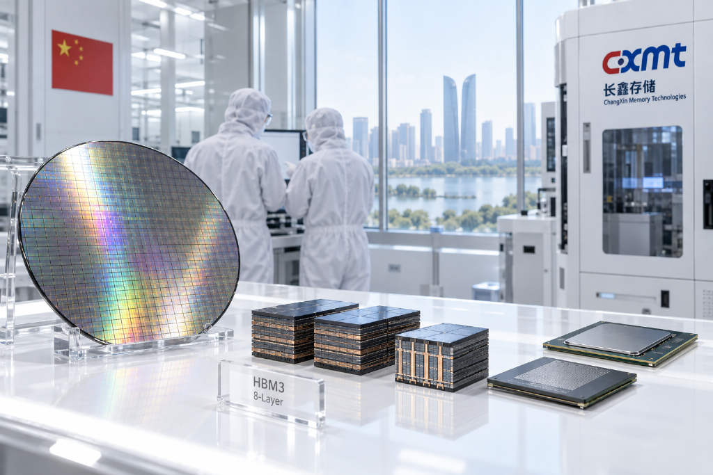
Chinese DRAM maker ChangXin Memory Technologies, or CXMT, has started pilot production of fourth-generation high-bandwidth memory HBM3, with initial yields stalled at 25%, according to a report by The Chosun Daily cited by ChainCatcher. The report said that level is roughly one-third of the 80% yield often seen as a target for mass production. SK Hynix has been mass-producing similar products since 2022, with yields above 90%.
For CXMT’s 8-layer HBM3 stack, front-end process yields were reported at about 30%, while roughly 70% made it through the back-end process as final good units. The company has supplied a small number of samples to Chinese firms including Alibaba’s T-Head and Cambricon, and is continuing to improve yields.
The report added that CXMT’s G4, a 17nm-class process, does not face major issues in conventional DRAM production, but HBM requires larger DRAM die and tighter electrical specifications. Industry sources in the report pointed to limited maturity in through-silicon via, or TSV, technology. Analysis from Nomad Semi said Samsung’s HBM2 has more than 5,000 TSVs per chip, SK Hynix’s HBM3 has more than 8,000, and CXMT has about 3,000, leaving the company 4 to 5 years behind Samsung and SK Hynix.
ChangXin Memory Technologies (CXMT), China’s largest DRAM maker, has started pilot production of fourth-generation high-bandwidth memory HBM3, with initial yields stalled at 25%, according to The Chosun Daily in a report cited by ChainCatcher.
The report said that figure is roughly one-third of the 80% yield commonly regarded as a benchmark for mass production. SK Hynix has been mass-producing comparable products since 2022, with yields above 90%.
For CXMT’s 8-layer HBM3 stack, front-end process yields were reported at about 30%, while around 70% became final good units after back-end processing. The company has supplied a small number of samples to Chinese firms including Alibaba’s T-Head and Cambricon, and is continuing to improve yields.
The report added that CXMT’s G4 17nm-class process does not show major issues in standard DRAM production, but DRAM chips used in HBM are larger in area and subject to tighter electrical specifications.
Industry participants cited in the report pointed to insufficient maturity in through-silicon via (TSV) technology. Analysis from Nomad Semi showed that Samsung’s HBM2 has more than 5,000 TSVs per chip, SK Hynix’s HBM3 has more than 8,000, and CXMT has about 3,000. The report said CXMT remains 4 to 5 years behind Samsung and SK Hynix.
This article was originally published by Bit.Fan. For more cryptocurrency news and market insights, visit www.bit.fan. Disclaimer:
The market information, project data, and third-party content displayed on this platform are for industry information sharing only and do not constitute any form of investment advice or return commitment.
Cryptocurrency trading carries high risks. Users should fully assess their risk tolerance and make independent decisions. All profits, losses, and legal responsibilities are borne by the users themselves.