
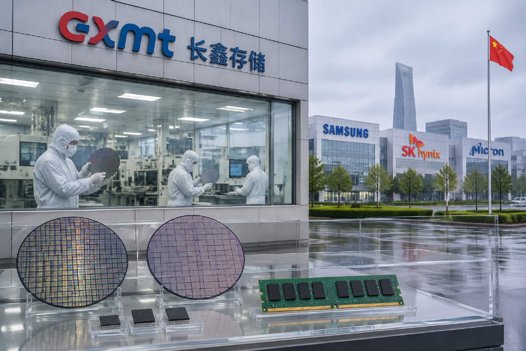
The DRAM industry is splitting over the 4F² route. After ChangXin Memory Technologies disclosed progress on its next-generation 4F² architecture and related products, Samsung Electronics said it is continuing parallel development, SK hynix signaled a gradual transition, and Micron Technology said it is not adopting the approach in its current roadmap.
The divide is about more than technology. Cost, yield, production ramp, and timing for commercialization are all part of the calculation. In its prospectus, CXMT described 4F² as one of its chances to overtake rivals on a curve, arguing that both the company and the three major overseas DRAM makers are still in the exploration stage and that large-scale commercialization remains uncertain.
Why 4F² is back at the center of DRAM competition
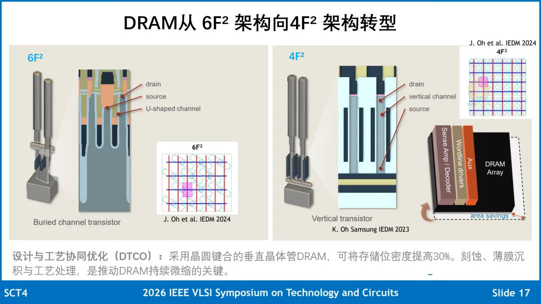
One of the core goals in DRAM process competition is to raise bit density per unit area. The theoretical planar footprint of a single DRAM memory cell can be simplified as kF². Under that framework, there are two main ways to improve density: reduce the layout coefficient k, or shrink the feature size F.
Roughly two decades ago, the industry compressed cell area from 8F² to 6F² by changing memory-cell layout. After that, density gains came mainly from continued scaling of feature size. Now that planar scaling is becoming harder, architectural innovation through a lower k is back in focus.
Moving from 6F² to 4F² would reduce the theoretical planar area of a memory cell from the typical 3F×2F layout to 2F×2F. In theory, at the same feature size F, that cuts cell area by one-third and increases the number of cells that fit in the same area by 50%.
Even so, the industry has not reached a common view on the technical feasibility, economics, or commercialization timing of 4F². That lack of consensus has created an unusual opening for a challenger.
CXMT is treating 4F² as a chance to catch up
From its first paper on 4F² architecture in 2021 to further discussion of technical challenges at IMW 2026, the IEEE International Memory Workshop, earlier this year, the market has known that CXMT was placing a heavy bet on the route.
What changed the tone was the speed of its product progress. On Oct. 10, CXMT said it expects to launch by year-end a next-generation DDR5 RDIMM product that combines 4F² architecture with hybrid bonding technology. The company said the pace of volume production will depend on customer validation progress and market demand.
That announcement sent shares of Samsung Electronics, SK hynix, and Micron sharply lower, though the article notes that a broader cooling in the AI narrative was also a factor.
For CXMT, 4F² is not just a technical experiment. It is also a route shaped by practical constraints. Without access to advanced lithography capabilities such as EUV, staying on the 6F² path would require continued shrinking of feature size F and rising dependence on DUV multi-patterning, putting pressure on economics through overlay precision, process window limits, and yield.
If the structural advantages of 4F² can be realized in production, CXMT may be able to use a relatively larger feature size F and reduce reliance on extreme lithography and repeated patterning. The article argues that, under that scenario, mass-producing 4F² DRAM could prove more cost-effective than continuing to scale 6F² through DUV multi-patterning.
Samsung stays engaged, SK hynix stresses timing, Micron says no for now
On Oct. 14, at an industry exhibition, Song Jaehyeok, chief technology officer of Samsung Electronics' Device Solutions division, confirmed that Samsung is working on 4F² architecture. Earlier this year, the company had already shown a 16Gb 4F² DRAM test chip using the related technology. According to the article, mass production is planned for 2028.
On Oct. 21, Micron President and Chief Technology and Products Officer Scott DeBoer said publicly that the company will continue extending the 6F² architecture while also advancing 3D DRAM research, and that 4F² is not part of its current technology path. The article says Micron was an early mover on 6F² and has studied 4F² for more than 20 years, but now sees the direction as expensive, difficult, and lacking a sufficiently attractive path to scale.
On Oct. 28, SK hynix said on its earnings call that it will transition to 4F² architecture, but that this is not the company’s focus at the current stage. Its present R&D plan is to rely on process maturity and a stable technology platform to extract as much value as possible from 6F² and extend the life of that platform. SK hynix said each technology should be applied to the right product at the right time, and that the right time includes both technical readiness and economic readiness.
Those positions line up with CXMT’s own assessment in its prospectus: 4F² remains in the exploration stage, and uncertainty still stands between the technology and large-scale commercial deployment. Differences in scaling capability, process environment, and cost structure are leading companies to different strategic choices.
The challenge is not just density on paper
Shifting from 6F² to 4F² is not a simple matter of shrinking cell area. It requires a redesign of the DRAM cell’s 1T1C structure. The new layout must preserve storage performance while also meeting yield, reliability, and cost targets.
Over more than 20 years of two-dimensional scaling, the capacitor, or C, has been stretched into a tall, narrow cylinder so it can still hold enough charge in a smaller space. To move from the typical 3F×2F layout of 6F² to the 2F×2F layout of 4F², the transistor, or T, would also need to stand upright, implying new device structures and integration processes.
Micron’s concern, as described in the article, is that while transistor layout can change, capacitors cannot be pushed arbitrarily close together because capacitance, insulation performance, and manufacturing reliability still have to be maintained.
That means the theoretical density gain of 4F² is likely to be reduced once capacitor spacing constraints, peripheral circuit area, and redundant cells are taken into account, even as process costs rise. On that basis, whether 4F² is economically superior to continued 6F² scaling is far from obvious. Even if development goes well, yield improvement and production ramp speed could weigh on profit for a long period.
Why incumbents may prefer to keep extracting value from 6F²
The article says the market remains hungry for DRAM. It even cites Sam Altman’s controversial question about why so much memory should sit idle in personal computers. Micron believes shortages will last through 2028, while SK hynix expects them to continue to 2030.
In that setting, for companies that already hold larger market share, committing large amounts of capital and R&D resources to a 4F² path with uncertain commercial prospects is not the most attractive option right now.
Those companies have EUV, or extreme ultraviolet lithography, and can keep improving density by shrinking F. That gives them room to squeeze more value out of 6F² during a period of high DRAM premiums. The article also notes that Micron was the last among the three to introduce EUV into DRAM mass production, but that its process experience from the DUV multi-patterning era laid the groundwork for that transition.
Why 4F² matters more for CXMT and China’s supply chain
CXMT faces a different set of constraints. Without EUV and similar advanced lithography tools, continued scaling along the 6F² path would mean deeper reliance on DUV multi-patterning, with higher cost and manufacturing difficulty.
4F² could change that equation. If higher density can be achieved at a relatively larger feature size F, dependence on extreme lithography may be reduced. The article frames that as a potential time window for the development of domestic advanced lithography equipment.
That is also why, while Chinese semiconductor companies are studying next-generation technologies such as 3D folding and 4F² alongside global peers, they may move earlier and more aggressively to push those technologies from the lab into products. The article’s point is simple: they do not have the same fallback options, and they do not carry the same historical burden.
4F² is not the endpoint for DRAM
Even so, the article argues that the move from 6F² to 4F² offers only a one-time structural gain. Once cell area is compressed to 4F² by changing the layout coefficient k, further increases in DRAM density still depend on continued shrinking of feature size F.
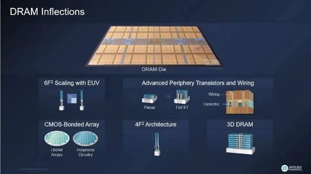
In that sense, 4F² is not the long-term endpoint for the DRAM industry, and it may not even evolve to 2F². Instead, it is presented as a transitional option in the search for next-generation memory architectures. Applied Materials’ DRAM roadmap, as cited in the article, includes not only 4F² but also scaling driven by advanced lithography, advanced peripheral transistors and interconnects, CMOS-bonded arrays, and 3D DRAM. These directions are not mutually exclusive.
Over the longer term, 3D DRAM is described as a key route for breaking through the density limits of planar arrays. Unlike 4F², which changes the layout inside a 1T1C memory cell, 3D DRAM stacks multiple 1T1C memory arrays vertically.
Pursuing 4F² could create a path to commercialization while also building experience in devices, materials, and process technology for future 3D DRAM. Skipping 4F² means betting that 3D DRAM can reach volume production before the economics of 6F² scaling run out, avoiding heavy investment in a transitional architecture with limited upside. The risk, in that case, is a technology gap lasting several years between generations.
Spillover effects beyond DRAM itself
For CXMT and China’s semiconductor supply chain, the significance of 4F² goes beyond DRAM. If the route keeps moving forward, R&D and manufacturing demand around the architecture would reach EDA, semiconductor equipment, and materials earlier.
At a stage when EUV capability remains constrained, the article sees this path — downstream chip architecture innovation pulling upstream supply-chain iteration — as one of the important ways for China’s domestic computing industry to address technology bottlenecks.
The article was originally published by the WeChat public account Weijin Research and credited to Weijin Research.