
The story around glass substrates is no longer about who announces first. It is becoming a test of who can deliver on time.
That shift came into sharper view in the second half of 2026. In late July, Intel and Lens Technology moved ahead with cooperation on glass-substrate packaging aimed at the AI era. On Aug. 11, South Korean equipment maker Avaco and affiliate AVAT EC started a pilot line for TGV process verification. A day later, supply-chain information indicated that Samsung Electro-Mechanics had run into a bottleneck in customer sample reliability testing, with the buildout plan at joint venture GlaSSEM potentially delayed and mass production possibly moving to after 2028.
Those developments point in different directions on the surface, but they reflect the same underlying reality. Glass substrates have moved beyond a phase centered on comparing material properties and into an engineering stage where customer reliability qualification sits at the center. What matters now is not simply the theoretical edge glass may have over organic substrates. The issue is whether glass can still maintain flatness, low warpage, and stable conductivity after drilling, copper filling, routing, and chip mounting, while also passing thermal cycling, humidity, and other reliability checks.
The exact tests and thresholds vary by customer specification. The process itself, however, cannot be compressed by capital spending or market excitement, and that is the core reason production schedules have been adjusted across the sector.
Samsung Electro-Mechanics shows how the bottleneck has shifted
The delay tied to Samsung Electro-Mechanics follows a timeline that stretches across nine months. Supply-chain information circulating in the market indicates the company had already communicated equipment purchasing intentions for the GlaSSEM production line to suppliers in November 2025. The order timing then moved from December 2025 to March 2026, then to June, with no fresh milestone disclosed after that point. Key suppliers for coating, etching, laser drilling, and inspection were largely identified, but orders did not land.
That does not suggest a lack of willingness to invest. In early July, GlaSSEM signed a final agreement with Dongwoo Fine-Chem, a unit under Japan’s Sumitomo Chemical. The joint venture has registered capital of KRW 482.1 billion, and Samsung Electro-Mechanics holds 66%. The public target is to establish the company in 2026 and build a supply system in the second half of fiscal 2027. That is not the same thing as full-scale mass production. Equipment lead times, the specific line-building pace at the Pyeongtaek plant, and the eventual production schedule still depend on customer qualification and equipment ramp-up.
The real sticking point appears to be samples. Current supply-chain information points to the customer-side sample reliability review, but the company has not publicly disclosed the specific test items, failure mechanisms, or customer identities involved. The path widely understood by the industry is to adjust the glass formulation and TGV drilling parameters, submit samples again, and complete a fresh full-process customer review. The key question for glass substrates is no longer only whether microvias can be drilled. It is whether the substrate can avoid cracking and keep performance intact after thermal stress from chip mounting.
Samsung is not alone. The commercialization pace at SKC and its U.S. subsidiary Absolics has also shifted. Market expectations now point to final reliability testing being completed in 2026 and full production being pushed in 2027. SKC has confirmed that its glass-substrate business is preparing for customer reliability evaluation and plans to produce related samples while reviewing projects under discussion with multiple customers. It has not formally disclosed customer names, final certifications, or mass-production orders. That distinction matters. Laboratory feasibility is one thing; stable yield and customer qualification are another.
The production calendar keeps moving right
Current schedules across the industry remain cautious. Absolics now expects to complete reliability testing in 2026 and push ahead with full production in 2027, later than earlier market expectations. GlaSSEM is targeting the second half of fiscal 2027 for supply-system establishment, while the exact timing for mass production is still uncertain. Dai Nippon Printing has already built its TGV pilot line and is aiming to put in place the systems needed for full mass production in fiscal 2028. LG Innotek had previously put mass production in the 2027-2028 range, but the commercialization pace still depends on technology progress and demand development. TSMC sees 2026 as an important window for CoPoS equipment and material verification, while market views still differ on later trial-production and volume-production timing. Lens Technology has disclosed pilot-line construction, sample fabrication, and customer technical testing, but volume output still depends on later agreements and qualification work.
Industry research groups are also keeping expectations in check. One view is that TGV glass substrates may not enter the mainstream of advanced packaging until after 2030 and are still in an early validation phase, serving as a supplement rather than a full replacement for existing packaging routes. Some domestic Chinese institutions are more constructive on the timetable, viewing 2027-2028 as the first industrialization verification window and projecting small-batch shipments from 2027, followed by a faster ramp in 2028. Those are forecasts and estimates, not achieved industry facts.
A delayed timetable does not mean demand has vanished. Public materials show that AI infrastructure and high-performance computing are increasing demand intensity for high-end IC packaging substrates, and manufacturers are expanding capacity at the same time. The fact that conventional substrate demand is growing even while glass-substrate production is being delayed suggests the bigger constraint sits on the supply side, in technical maturity, rather than on whether downstream demand exists. The market is not looking for another material that looks better on paper. It needs one that can be delivered consistently under large-format, high-layer-count, high-frequency interconnect conditions.
Intel and Lens Technology: more than a simple order story
The Intel-Lens Technology cooperation is worth reading carefully. According to Lens Technology’s disclosure, the two sides signed a memorandum of understanding focused on TGV advanced packaging. Lens Technology is responsible for through-glass via formation, high-precision laser processing, metallized via deposition, and multilayer interconnect routing. Intel is expected to provide explanatory architecture information, design-for-manufacturability guidelines, benchmark testing, and validation methods.
The significance lies less in a single order and more in how qualification systems begin to extend outward. If the design side is willing to provide DFM rules and validation methods, the glass-processing side can enter the design loop for real packaging architectures earlier than before.
There is a practical basis for that arrangement. Lens Technology has said it built relevant pilot lines, carried out sample trial production, and delivered samples to some potential customers. Some customers passed preliminary proof of concept and moved into technical testing. The market has also circulated figures tied to a pilot line with monthly capacity of 3,000 units, zero-ppm open-circuit rates across million-scale vias, minimum apertures below 10 microns, a 30,000-square-meter dedicated TGV facility, and joint verification of a 22-layer glass core substrate. Until the company provides further disclosure, those figures should not be treated as confirmed mass-production facts.
The MOU also should not be read as a binding order. Lens Technology stated clearly that whether a formal agreement will be signed remains uncertain, and as of the announcement date the TGV business had not had a material impact on operating results. From an industry standpoint, this looks more like a move to secure capability positioning. From a financial standpoint, there is still distance before it turns into measurable incremental business.
Japan is advancing validation first, while Chinese companies accelerate entry
The contrast between Japanese and Chinese companies helps explain the diverging production calendars.
In July, Shinko Electric Industries showed a 22-layer glass core substrate with 11 layers of copper routing stacked on each side of the glass. The technical focus was not only the layer count. The company also emphasized the use of protective material at substrate edges to disperse thermal stress and suppress SeWaRe defects, meaning internal cracking and delamination that can appear during processing or thermal cycling. Dai Nippon Printing, for its part, launched a TGV glass core substrate pilot line in Saitama in December 2025 and is targeting fiscal 2028 for the systems needed for full production. In both cases, public milestones are centered on multilayer routing, thermal-stress control, and pilot validation rather than broad mass-production declarations.
Chinese companies are entering from a somewhat different angle. In August, an industry research institution listed 18 Chinese listed companies participating in the glass core substrate supply chain, spanning specialty glass, TGV processing, metallization, and advanced packaging. BOE’s disclosed progress is one of the clearer examples. Its glass-based packaging substrate test line achieved full automation equipment linkage in the first half of 2026, with designed capacity of 1,000 units per month. The company has completed development and sample delivery for large-size, high-layer-count glass-based substrates, and some domestic customers have entered the technical testing stage. Even so, the business has not yet reached mass production and has not generated mass-production revenue.
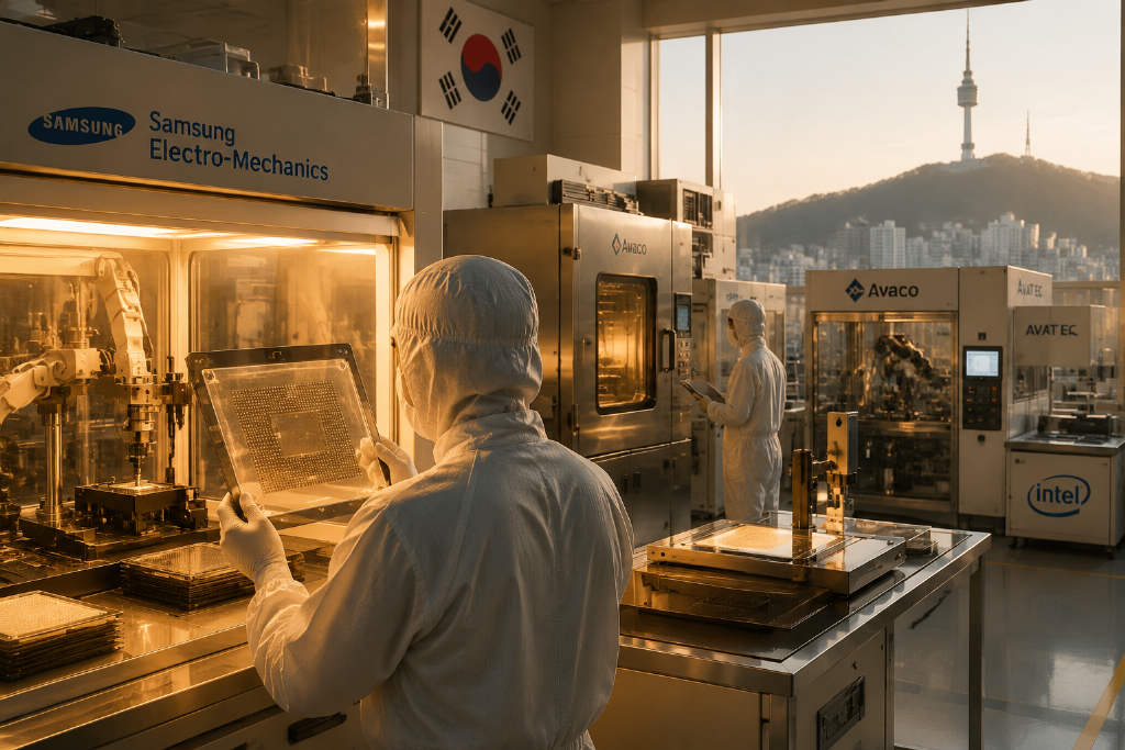
Equipment-side verification is also moving forward. The TGV pilot line launched by Avaco and AVAT EC supports large-format glass at 515 x 510 mm and links together laser drilling, etching, seed-layer deposition, and optical inspection. Its importance does not come from immediate scale. It comes from testing repeatability and process handoff efficiency across multiple critical steps for large-format glass. Japanese materials and substrate companies, Chinese panel makers, and South Korean equipment suppliers are all moving toward the same end point: turning glass-processing capability into a repeatable semiconductor manufacturing capability that can survive customer qualification cycles.
Schott and Corning push glass toward optical interconnects
Material makers are showing that the value case for glass substrates is not limited to replacing ABF. Schott has publicly introduced glass substrate and advanced packaging products aimed at high-density TGV, advanced heterogeneous packaging, and high-performance interconnects. The product positioning emphasizes different coefficients of thermal expansion, thicknesses, and electrical characteristics to meet the material demands of high-performance packaging.
Corning’s direction may be even more representative. The market’s focus on the Glass Bridge concept centers on using TGV in next-generation co-packaged optics, or CPO, designs so glass extends from packaging substrate into optical interconnect substrate. Corning and Nvidia have signed a multi-year commercial and technical cooperation agreement, with the official disclosure focused on expanding optical connectivity and fiber manufacturing capacity in the United States. That cooperation itself should not be directly described as a glass-substrate or Glass Bridge project. Earlier, BOE and Corning signed a three-year memorandum of understanding covering glass-based packaging substrates and optical interconnects.
This changes how the first application wave is being viewed. Nvidia has publicly discussed the CPO technology path, while Broadcom has described the second-generation Tomahawk 5-Bailly as the industry’s first production CPO solution. That suggests the CPO ecosystem is entering a more concrete engineering phase. Compared with the longer industrialization cycle for glass-core packaging substrates, glass optical interconnect substrates aimed at CPO may offer an earlier landing point. Intel has also positioned glass as a foundational technology capable of integrating electrical and optical functions on the same platform.
The material barriers remain substantial. Glass materials, TGV formation, metal filling, low-loss routing, thermal-expansion control, and large-format manufacturing all involve patents and accumulated process know-how. As the industry matures, licensing and process-route choices may become new competitive variables.
Yield is the only hard currency
Under every debate about schedules sits the same engineering problem: TGV yield. TGV is the process of drilling tiny vertical vias into glass with lasers and filling them with copper to carry electrical signals. Each substrate requires thousands of these vias to be aligned precisely in a brittle material. Current glass-core packaging yield is around 60% to 70%, well below the 80% to 90% range for organic ABF substrates. Because glass is brittle, even a small crack from laser drilling can scrap the entire substrate, pushing costs 30% to 50% above ABF.
MarketsandMarkets projects the global glass-substrate market will reach $8.4 billion in 2028. Sigmaintell Consulting has given a close estimate of $8.5 billion, with the market potentially reaching $27.6 billion by 2030. Those figures depend on a major improvement in yield and qualification over the next two years.
The burst of developments seen in the summer of 2026 amounts to the first real industrial exam for glass substrates as they move from the lab to the factory floor. The exam is not over yet, but the passing line is already clear.
This article was sourced from the WeChat public account "Semiconductor Industry Review" (ID: ICViews) and written by Junxi.