



At Hot Chips 2026, Samsung and SK Hynix agreed on the same premise: GPUs, memory, foundry technology and packaging now need to be designed as a single system. From there, their roadmaps diverged.
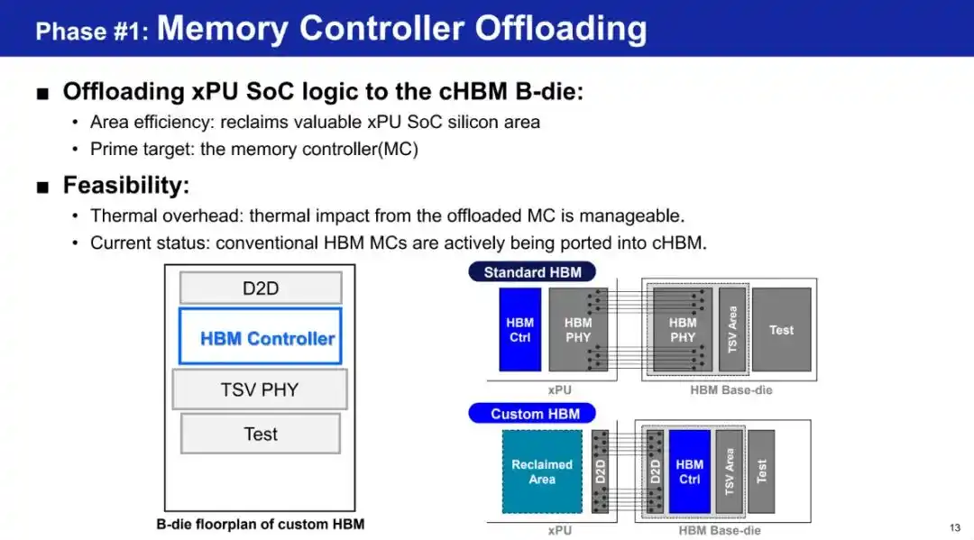
Samsung is trying to turn the HBM base die from a passive transport layer into an active part of the system. It plans to move the memory controller off the GPU and onto a logic base die, which it said could free up 5% to 10% of GPU area for more compute and potentially improve performance by 10% to 20%. Select AI operations could also run on the base die to cut data movement. Longer term, Samsung is pushing zHBM, a concept that stacks GPU and DRAM directly in a true 3D structure, with a target of cutting DRAM power by about 70% and delivering more than 2.3x the bandwidth of HBM4E.
SK Hynix is taking a different route. Its focus is on taller stacks and on managing the thermal load and warpage that follow. The company said 12-high HBM4 has entered production and 16-high versions are in customer validation. Hybrid bonding, in its view, is the path to 20-high and beyond. SK Hynix also introduced iHBM, which adds a dedicated heat-conduction path inside the hottest area of the stack. The contest is no longer just about bandwidth and capacity. Base-die architecture and advanced packaging are now central to HBM competition.
Samsung’s roadmap turns the base die into an active logic layer
In its Hot Chips 2026 presentation, Samsung Electronics introduced zHBM as what it described as the end-state evolution of High Bandwidth Memory. The concept removes the 2.5D interposer and vertically stacks DRAM directly on top of compute chips such as GPUs, creating a true 3D integrated architecture. Samsung’s stated target is a 70% reduction in DRAM power and bandwidth that is 2.3x higher than HBM4E.
Samsung laid out a three-stage roadmap. Stage one moves the memory controller from the xPU to the base die to reclaim silicon area. Stage two adds memory expansion and attention-compute capability to the base die. Stage three is zHBM itself.
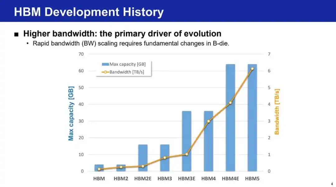
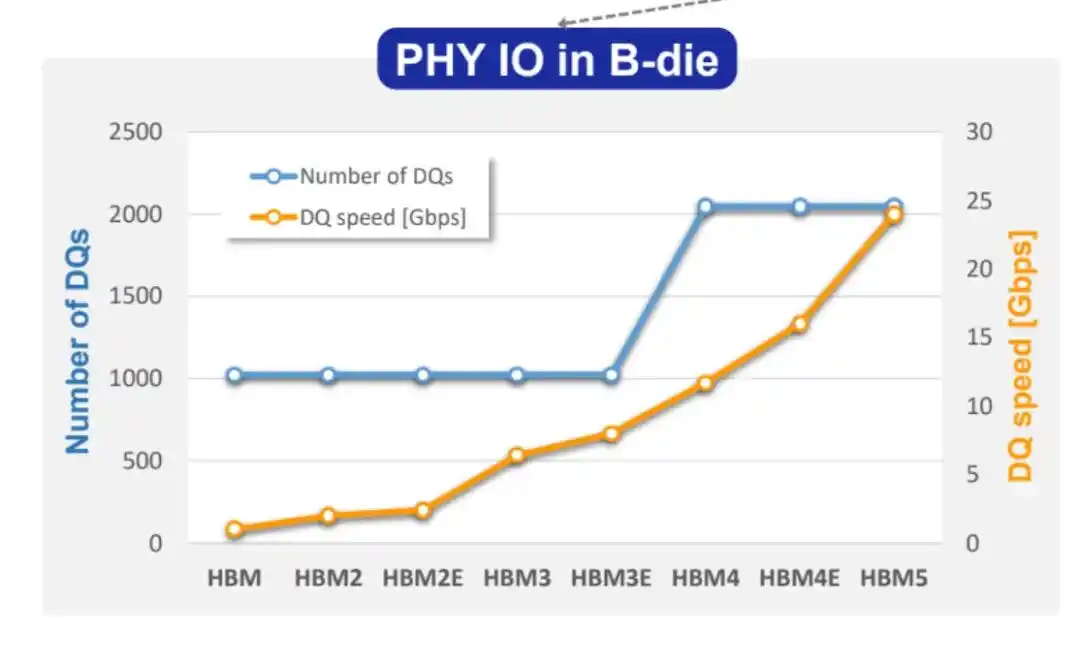
The company also showed trend charts for HBM5 specifications. Based on the figures cited in the source material, a 60 GB HBM5 stack delivering 6 TB/s across 2,048 channels implies per-pin data rates of about 23.5 Gbps. The same source says the most advanced speed currently in hand is 16 Gbps, and Samsung separately confirmed 16 Gbps per pin for HBM4E. At 3 GB per die, a 60 GB device would require a 20-high stack.
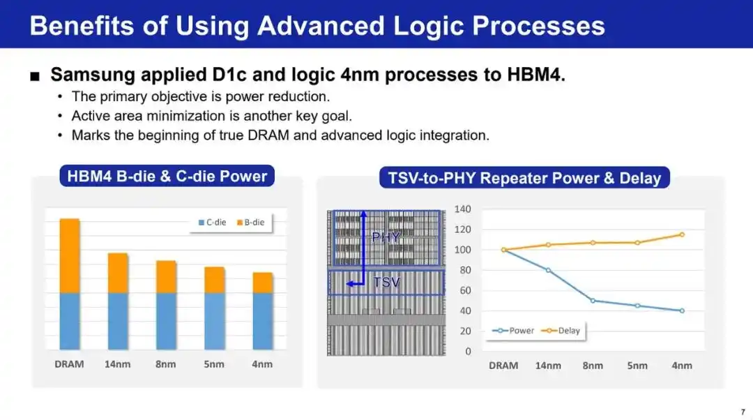
Samsung argued that one of its structural advantages is in-house logic capability. The source states that Micron and SK Hynix need outside cooperation for that class of die, while Samsung can pair 1C process technology for memory with a 4 nm process for logic, reducing power. Samsung used that point to make the case for custom logic base dies.
Stage one: smaller PHY, more compute area, higher thermal density
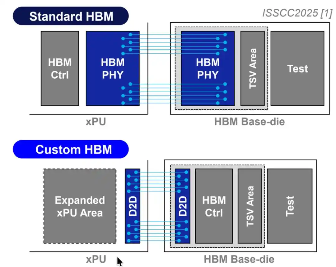
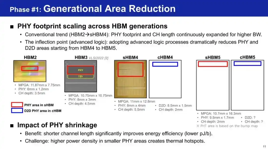
Samsung said a logic-node base die shrinks the physical size of the HBM PHY and improves energy efficiency. That reduces the size of the die-to-die interface between HBM and the xPU. The gain shows up in two places: more area on the xPU for compute, and more usable area on the HBM base die for added functions.
The trade-off is heat density. Smaller interface regions run hotter, not cooler. Samsung showed actual PHY sizes across different HBM generations and, for the transition toward HBM5, proposed an integrated Heat Path Block, or HPB, to cool the D2D PHY region.
Samsung also said it does not favor UCIe for this D2D link because UCIe is larger and consumes more energy per bit. In its presentation, the company said its custom PHY implementation performs better.
Another direct benefit comes from offloading the memory controller. Once the controller moves to a custom base die, space on the xPU can be repurposed for more floating-point compute units.
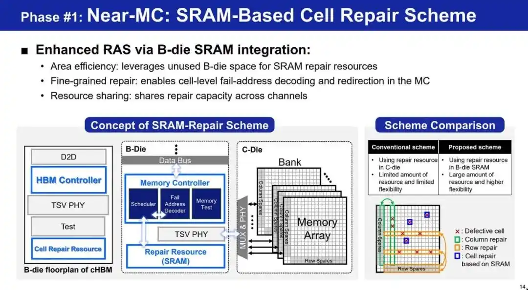
A logic base die also makes it possible to integrate SRAM. The source gives a concrete example: if a cell in the DRAM stack fails, the affected data can be held temporarily in SRAM, and the memory controller can retrieve it from there rather than from the damaged DRAM cell.
Stage two: RAS, testing, telemetry, expansion and selective compute
In Samsung’s second stage, the point of using a smaller-transistor logic node is not just area reduction but function density. The freed-up silicon can be used for repairability, availability and serviceability, testing, and telemetry on the health and status of the HBM stack.
The source material says HBM telemetry is the second-largest cause of training failure, which is why Samsung sees practical value in integrating that capability. If there is still spare die area, Samsung’s roadmap also adds a memory expansion controller so another HBM stack, or separate DRAM, can sit behind the first stack to increase memory capacity.
From there, Samsung extends the idea to selective compute on the base die itself. Tasks such as matrix compression or encoding could be handled locally on the logic die instead of sending data out of the stack. That could improve latency and efficiency. The source also notes that while the block diagram is conceptually elegant, the real-world size of the performance gain remains open to question.
Stage three: zHBM and vertical integration
The final stage is verticalization. Samsung’s plan is to stack the custom base-die HBM structure directly on top of the logic chip. That shortens the distance between compute and memory, which improves energy efficiency. It also creates room for more parallel data paths across the die area, not just around the die edge, lifting memory bandwidth.
The source describes this as a difficult path, but an important one to chart. It signals that Samsung has a defined route for future product improvement. Whether the market is ready for that product form is a separate question.
SK Hynix is pushing taller HBM stacks and the packaging needed to hold them together
Jaesik Lee, vice president of packaging engineering at SK Hynix America, said on Aug. 23 at Hot Chips 2026 that hybrid bonding is not expected to meet HBM4E requirements. That means the industry’s most watched memory-packaging transition may not arrive before HBM5.
As Lee explained, the total thickness of an HBM cube is capped at 775 micrometers, which matches the standard thickness of a 300 mm logic wafer. Every additional DRAM layer therefore forces thinner dies and smaller gaps. The 16-high dense HBM4 now in customer qualification, carrying 48 GB per cube, trims core-die thickness to about 50 micrometers and cuts inter-die spacing in half. SK Hynix also said 12-high dense HBM4 is already in production.
The source says JEDEC raised the HBM4 package-thickness limit to 775 micrometers from the 720-micrometer cap used for HBM3E. That eased some of the pressure to move immediately to hybrid bonding. Lee said that when GPU packages are prepared for cold-plate mounting, part of both the logic die and the memory stack is ground away to expose bare silicon. If the memory stack grows any taller, it can exceed the height of the processor next to it. “This is the limit we can raise to right now, because the logic wafer thickness is also 775 micrometers,” Lee said.
Thinner dies bring thermal penalties. They increase the fraction of oxide in the stack, and oxide conducts heat less effectively than silicon. At the same time, per-pin speed has climbed from 1 Gbps in early HBM generations to 8 Gbps in HBM4, raising power consumption in the same area. SK Hynix data shown in the source indicates an average 2.2x increase in thermal load across the HBM generations discussed, while stack height doubles every two generations.
Its mass reflow molded underfill process, or MR-MUF, stacks all dies through pick-and-place and then bonds them in a single reflow step. Lee said the main manufacturing challenge for 16-Hi is filling gaps that have been cut in half while controlling warpage in dies thinner than 50 micrometers.
Hybrid bonding remains an R&D path for 20-high and above
The source recounts that Samsung publicly committed in May last year to produce HBM4 with hybrid bonding, while SK Hynix positioned copper-to-copper bonding as an alternative to advanced MR-MUF. JEDEC later relaxed thickness limits, reducing the urgency. The industry is now discussing lifting the thickness allowance for 20-high stacks to 825 to 900 micrometers, which could delay broad adoption of copper bonding again.
The source also says industry claims surfaced in March that SK Hynix placed its first mass-production hybrid-bonding order, a single-line system worth about KRW 20 billion, or $15 million, combining tools from Applied Materials and Besi. Counterpoint Research expects the technology to enter full HBM production around 2029 to 2030 with HBM5.
According to SK Hynix’s roadmap, hybrid bonding is still in the R&D stage and is aimed at stacks of 20 layers or more. The company has not decided which product will use it first. Lee did not name the generation, but once HBM4E is ruled out, HBM5 appears to be the earliest candidate. The process bonds flat copper pads and oxide surfaces at room temperature, then relies on copper’s thermal expansion during curing to complete the connection.
“This seemingly simple process is actually very challenging,” Lee said. “We need 16 layers or even 20 layers to realize hybrid bonding, which is completely different from single-layer stacking.” The source says removing microbumps entirely would allow the core die to be 24% thicker at a 20-high stack height, reduce thermal resistance by about 35% compared with MR-MUF at the same height, and push bump pitch below 18 micrometers, versus 30 micrometers for MR-MUF today.
That said, conventional microbumps remain viable at HBM4 bump pitch, and every time JEDEC lifts the thickness limit, MR-MUF gains more room to extend into the next generation.
iHBM targets package-internal hotspots
SK Hynix’s iHBM concept embeds a thermally conductive but electrically insulating block inside the inter-die PHY region of the base die, identified in the source as the interface hotspot with the highest power density. SK Hynix says that can reduce thermal resistance by more than 30%.
Lee’s slides directly compared iHBM with Samsung’s Heat Path Block approach. Samsung’s design uses dedicated thermal pillars to pull heat out of the stack, while Micron has claimed more than 20% efficiency gains from a redesigned base-die circuit. The source explicitly notes that all three are vendor claims measured under different standards.
Both SK Hynix and Samsung intend these designs for HBM5, but volume production is not expected before 2028. Lee said such modules sit inside the package with the D2D PHY chip and must be optimized around customer designs, which prevents them from being applied to already-designed chip generations. “This is a good option that we can do, but we cannot apply it to chip generations that have already been designed,” he said.
Q&A raised a harder question: does taller always mean better?
In the Q&A session, SemiAnalysis’ Tanj Bennett argued that taller memory stacks reduce silicon-level throughput. He said DRAM operating at the cell level delivers about 20 TB/s per square centimeter, while a 20-high stack tops out at around 4 TB/s. He also said HBM requires far more manufacturing capacity than equivalent DDR5 or LPDDR.
“When the stack height gets to 20 layers, the average speed of this memory is actually slower than DDR5,” Bennett said. “Why use the height of HBM stacking instead of placing cheaper memory around it more cleverly?”
Lee replied that training workloads need both bandwidth and capacity, while inference can split the hierarchy by keeping key-value cache in high-bandwidth memory and offloading part of the work to LPDDR. The source says that approach is already used in products such as Nvidia’s Vera Rubin platform, which pools LPDDR5X and HBM4 through NVLink-C2C for that purpose. SK Hynix and Sandisk are also jointly developing a high-bandwidth flash specification that extends the same tiered-memory logic to NAND flash.
Speaking about layered memory strategies, Lee said, “This is also something we need to consider in the future.” The source also says reports in January put SK Hynix at roughly 70% of Nvidia’s Vera Rubin-generation HBM orders, all using MR-MUF. The company still has not decided which product will adopt hybrid bonding first.
Micron says the AI memory wall is getting worse
Micron approached the same broader problem from another side, focusing on how memory architecture is evolving inside AI systems. The company presented HBM and advanced packaging as core elements of AI system design rather than add-on technologies.
Its talk opened with OpenAI’s compute-efficiency frontier theory to explain why memory matters for scaling language models. Micron said model size, dataset size and training compute follow a power-law relationship and need to scale together if language-model performance is to keep improving. Memory is the resource that links all three.
Micron’s central argument was that AI accelerator TFLOPS are rising about 3x every two years, while the bandwidth of 2.5D attached memory such as HBM is growing at less than 2x over the same period. That widening gap is what makes memory technology a key limiter on AI system performance.
The company positioned HBM as the bridge between compute and memory and walked through rising capacity, bandwidth and energy efficiency from HBM2e through HBM5. One slide showed a typical GPU package larger than 12,000 square millimeters, including the base die and eight HBM4 devices. With 12-high HBM4, the memory silicon area can exceed the GPU die area by more than 8x.
Micron also reviewed HBM’s progression from HBM1 to HBM4. Each generation increased data rate, pseudo-channel count and stack height, leading to more bandwidth and more capacity. Instead of coming as a socketed module like standard memory, HBM is integrated with a GPU or accelerator inside a system-in-package structure.
At the die level, each DRAM die contains multiple independent channels, and each channel has two pseudo-channels. HBM3E carries 128 banks per die, while HBM4 doubles that to 256. The base die sits between the host and the DRAM stack, using a microbump PHY on the host side and a 3D TSV PHY on the stack side, connected through a high-density point-to-point interposer link that scales from 1K I/O in HBM3E to 2K I/O in HBM4.
The cost side is heavy. Micron said the combined complexity of architecture, advanced packaging and manufacturing means HBM3E requires about three times as much silicon as DDR5 to reach the same memory capacity.
On packaging, Micron pointed to faster I/O links and larger interposers as the drivers of continued system-in-package progress. It cited faster I/O design, memory-optimized SERDES and chip-to-chip PHY, co-packaged optics on the interconnect side, larger SiP structures based on CoWoS-L and CoWoS-R, and glass substrates as part of the path forward.
Reliability is another constraint. In heterogeneous HBM devices, mismatches in thermal expansion coefficients across materials create thermomechanical stress. ECC protection is split into two layers: a system-level scheme in HBM3 that uses 16 meta-bits per 256-bit access, and an on-die symbol-based Reed-Solomon ECC implementation.
Thermals close the loop. Micron said rising DRAM activity, taller stacks and more capable base-die logic all add heat. Liquid cooling, hybrid bonding, and improvements in solder and side molding are among the thermal-management tools needed to preserve the path to higher bandwidth and capacity.
Taken together, the presentations point to the same conclusion without offering the same answer. HBM still has room to scale, but every step forward in bandwidth and capacity now comes with deeper trade-offs in packaging, cooling, reliability and silicon cost. Samsung, SK Hynix and Micron are moving toward that constraint from different directions.
The source of the original article is the WeChat public account Semiconductor Industry Observation, author listed as Editorial Department.