
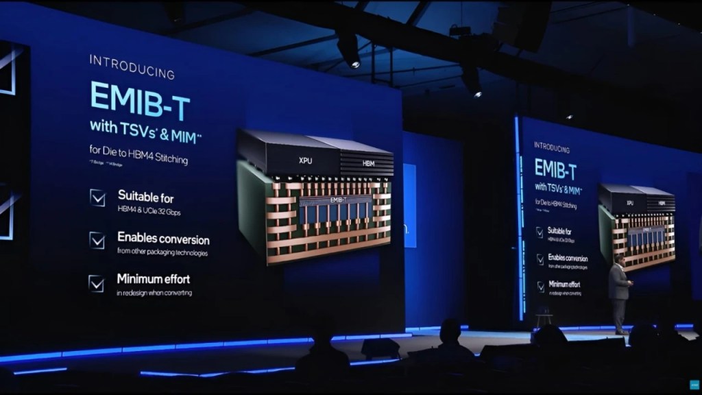
Intel’s EMIB-T advanced packaging technology is moving toward commercialization at a faster pace. According to industry information cited by ABMedia, packaging yield has climbed to nearly 90%, while total packaging cost is only about half that of Taiwan Semiconductor Manufacturing Co.’s CoWoS solution. The main constraint now sits on the substrate side. The report said Intel is aiming for formal mass production in 2027, a timeline that could put pressure on TSMC’s long-held position in advanced packaging.
How EMIB-T differs from CoWoS
Intel’s EMIB technology uses a miniature silicon bridge embedded directly inside an organic substrate instead of the large silicon interposer required by CoWoS. That structure allows multiple dies to be connected at high density inside a single package.
EMIB-T is an upgraded version of EMIB. Its key change is the addition of through-silicon vias, or TSVs, inside the embedded silicon bridge. Those vertical connections let power and high-speed signals travel from the bottom of the package, through the bridge, and up into stacked processors or memory, enabling what the report described as true 3D stacking capability.
Pricing is reported to be 40% to 50% below CoWoS
The cost advantage is central to the technology’s market case. ABMedia, citing a recent Digitimes report, said EMIB-T removes the need for the expensive silicon interposer that CoWoS depends on. As a result, overall packaging quotes are about 40% to 50% lower than CoWoS.
That gap matters for cost-sensitive customers developing ASICs or CPU-based AI chips. The report said EMIB-T’s packaging cost is roughly half of CoWoS, giving Intel a possible opening in AI chip packaging where supply and cost remain major concerns.
Packaging yield is near 90%, but substrate yield remains around 50%
ABMedia said the commercialization path is advancing quickly on the packaging side, while substrate manufacturing is still ramping. Packaging yield has reached close to 90%, a level the report described as sufficient for large-scale commercial production. Formal mass production is expected to begin in 2027, with Intel positioning EMIB-T to challenge CoWoS market share.
The larger issue is substrate yield, which is still at about 50%. The report described this as the only major technical bottleneck left to solve. EMIB-T substrates require a highly precise manufacturing flow and consist of three main layers:
- The organic substrate base, which houses the silicon bridge and requires precision drilling. Supply is led by Ibiden, with Shinko, Unimicron and AT&S also involved.
- A dielectric buildup layer laminated above the silicon bridge, using the industry-standard Ajinomoto build-up film, or ABF.
- The silicon bridge itself, which includes TSVs for vertical power delivery and signal routing.
Ohio fab work continues as Intel targets 14A production in 2031
At the same time, Intel is continuing construction of its large wafer fab complex in Ohio. The site spans more than 1,000 acres and is a key production base for the company’s Angstrom-generation process nodes, including 18A and 14A.
Wccftech said Intel has started paying overtime bonuses to workers on site in an effort to speed up construction. The stated goal is to reach large-scale production on the 14A node in 2031.
CoWoS supply tightness gives EMIB-T an opening, but hurdles remain
With CoWoS capacity remaining tight, the report said EMIB-T is gaining a clearer route into the AI packaging market. According to customer feedback relayed by Unimicron, the main reasons some customers are considering a shift from CoWoS to EMIB-T are lower cost and better performance. The primary target group is said to be ASIC vendors.
Even so, the expansion path is not free of risk. ABMedia said substrate yield still needs to improve, and the speed of the supply-chain ramp remains uncertain. Those factors are likely to shape EMIB-T’s commercial competitiveness and its level of market acceptance.