
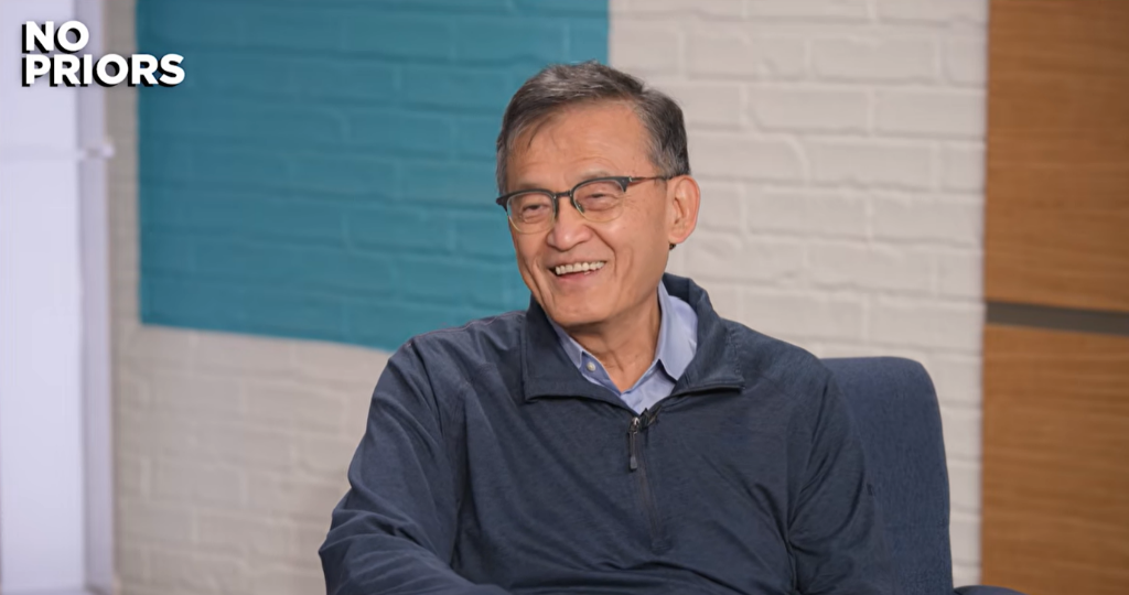
Intel CEO Lip-Bu Tan used a recent appearance on the No Priors podcast to lay out, in unusually detailed terms, how he is trying to remake one of the most important companies in the global semiconductor industry. Tan said Intel has already created roughly a 6x return for shareholders over the past 14 months, but described that as only the beginning. His stated personal target is a 10x return over the next five to ten years. In his view, the market will begin to see Intel’s full potential between 2030 and 2032, not only in its traditional PC client franchise, but also across edge computing, physical AI and agentic AI.
Tan, 66, came to Intel after a long career that included investing at Walden and leading Cadence as CEO. In the interview, he said the most surprising episode of the past year was a direct request from President Trump that he resign over alleged conflicts of interest. Tan said he first reminded himself that he did not need the job and had taken it because he wanted to save Intel. He later secured meetings, explained that he was born in Malaysia, grew up in Singapore, graduated from MIT and had lived in the United States ever since, and said he was grateful that Trump gave him the opportunity to continue.
Repairing the balance sheet and rebuilding Intel at startup speed
Tan described the first phase of the turnaround as cultural. He wants clearer accountability, faster decisions and fewer bureaucratic layers. Coming from a startup and venture-capital background, he said he is used to moving at what he called light speed, while Intel had become dependent on layers of meetings. From his first day, he decided that all engineering teams would report directly to him, because he wanted to know personally where the problems were and what needed to be corrected. Listening to customers, making customers satisfied, simplifying the product line and setting a five-to-ten-year roadmap form the operating base of his plan.
The balance sheet came first. Tan said Intel’s financial position was in poor shape when he arrived, and he welcomed the U.S. government becoming a major shareholder. He told President Trump that countries such as Japan and Singapore treat this type of manufacturing capability as infrastructure, and therefore government support has a clear rationale. He also thanked Nvidia CEO Jensen Huang, who invested $5 billion in Intel; Tan said that stake has now appreciated to $25 billion or more. SoftBank founder Masayoshi Son, with whom Tan had a board relationship, also provided support. These steps, in Tan’s telling, helped stabilize the company before the next product cycle.
On products, he said the surge in agentic AI and inference workloads has brought CPU demand back into focus. During training-heavy phases, the ratio of CPUs to GPUs in servers was around one to eight. Tan now sees that changing toward one to four, and in some cases even lower. He said AI model developers have told him that CPUs are especially useful in reinforcement learning and in coordinating and scheduling agents. That change gives Intel a timely opportunity to rebuild its data-center server lineup around workloads where CPUs again matter.
Packaging, glass substrates and new materials move to the center of the roadmap
Tan repeatedly returned to the same technical theme: traditional node scaling is getting more expensive and more difficult as it moves closer to physical limits. Intel has 18A, is pushing 14A toward mass production, and Tan said he can see paths to 10 nanometers and 7 nanometers in the roadmap language used in the interview. He also mentioned planning for 1 nanometer and 0.7 nanometer class processes. As line widths become extremely small, any mistake in manufacturing can undermine the whole process, which is why he emphasized close collaboration with substrate suppliers and equipment makers to improve yield and performance.
Advanced packaging is the second bottleneck he highlighted. TSMC has CoWoS, while Intel is pushing its next-generation EMIB technology. Tan said the key is making sure EMIB reaches the yield levels customers need in mass production. Intel has around 1,000 patents in modules, and the engineering challenge he identified is how to integrate substrates and modules effectively. Intel has also announced advanced-packaging manufacturing cooperation projects in India and in New Mexico in the United States.
Tan’s materials strategy extends beyond silicon. He said he has invested in gallium nitride, silicon carbide and indium phosphide companies, with some of those businesses already acquired by larger semiconductor companies including ADI. In packaging materials, he invested in 3DGS, a glass-substrate company, because he sees glass as a strong thermal and insulating material. He also invested in a synthetic diamond wafer company and sees diamond as another strong insulating material for chip packaging. As he put it, the engineering mindset is to keep encountering bottlenecks, then find a way to cross them or go around them.
Foundry discipline, trust and the Terafab partnership with Elon Musk
Intel’s foundry business has faced skepticism, but Tan said he chose to stay with it because advanced manufacturing in the United States has strategic value for supply-chain security. No major semiconductor company, he argued, should concentrate its supply chain in one or two geographic areas. In execution, he has narrowed the key metrics to yield, defect density and cycle time. Foundry, in his words, is a service business and a trust business: customers must trust Intel before they hand over wafers, and if poor yield causes revenue loss for a customer, that customer will be very hard to win back.
Tan also framed Intel and TSMC as partners rather than only competitors. He acknowledged that Intel still has a large gap to close in foundry and said the company must remain humble while strengthening IP, yield, defect density and cycle time. He also said the industry needs more capacity to serve growing demand. His timeline for the foundry business is long: he expects the real market recognition of Intel’s foundry potential to begin around 2030 to 2032.
The interview also covered Terafab, Intel’s cooperation with Elon Musk. Tan said he and Musk share the view that semiconductor infrastructure has not kept up with AI growth in capacity, production efficiency or power efficiency. Under the project, Musk decided to build his own fab, while Intel will provide technology and process support to help accelerate production. Tan said he meets with Musk’s team every week and described the collaboration as exciting. He also mentioned Musk’s habit of questioning convention, including a discussion about whether smoking could be allowed in some areas of a cleanroom. Tan said he would not go that far, but emphasized the need to keep an open mind and evaluate ideas seriously.
AI pressure points across power, helium, memory and design tools
Tan said AI will affect the global landscape more deeply than the internet. In semiconductor design, AI can improve timing optimization, speed time to market and reduce cost. At the same time, AI demand is running into multiple bottlenecks. Some countries do not have enough power. Helium has a significant impact on the semiconductor industry, an issue Tan said many people do not recognize. Memory shortage is the most urgent current constraint, and even if companies expand capacity now, new supply takes years to come online. CPUs and GPUs are also in short supply, pushing prices higher and eventually passing costs to clients.
Tan’s investor background shaped much of the conversation. He said his record includes 159 IPOs, 126 M&A exits and more than 200 semiconductor investments, with 38% of those in the United States. His investment framework begins with a simple question: where is the bottleneck, and what problem is being solved? He cited Cradle Semiconductor as an investment tied to the interconnect bottleneck, and Celestial AI as an example tied to the growing importance of optical interconnects inside clusters. He also noted that Jensen Huang has invested in nearly every photonics-related company, saying that is not a coincidence.
In EDA, Tan sees major opportunity in using AI and machine learning to reduce design complexity and improve design quality. He also highlighted new materials such as gallium nitride, silicon carbide and indium phosphide, some of which have led to acquisitions by companies such as ADI. Power management is another bottleneck he follows closely, especially the large losses involved in converting from 40V to 1V. When evaluating startups, he asks whether the customer pain is real and who the first target customer is, often preferring hyperscale customers that can pay millions over several years or provide some form of support if they like the product.
Talent was another recurring theme. Tan named the United States, Silicon Valley, Austin and Israel as areas he watches closely. He praised Israeli entrepreneurs for highly disruptive innovation and for continuing to hold meetings even during wartime, sometimes moving to a basement during an alert and switching to audio because the network connection is poor. Beyond agentic AI, he described physical AI as the next major frontier and said he remains deeply involved in investments tied to frontier models and open-source technology for physical AI.
Cadence lessons, capital strategy and Intel’s 10x ambition
Tan spent almost 15 years at Cadence and said one of his proudest achievements was identifying and developing his successor, who is now actively bringing agentic AI into design tools to improve efficiency. He said Synopsys CEO Sassine is pursuing a similar direction, supported by Nvidia’s $2 billion investment and by Synopsys’s acquisition of Ansys to extend into full-system design. Large companies are moving in this direction, but Tan said startups still have room to build more disruptive products, eventually choosing either IPO paths or acquisitions by the two large EDA companies depending on the founders’ ambitions.
On capital, Tan said capital-intensive infrastructure businesses require different funding sources. Some venture firms are now willing to put $1 billion into a single company, a level he said would have been hard to imagine in the past. For AI factories and foundries, he said companies need to seek support from government funds, sovereign wealth funds or large infrastructure funds. As the CEO of a public company, he also wants long-term investors rather than only short-term holders focused every quarter on buybacks, while still recognizing that shareholder return is a legitimate concern.
Asked about investor misunderstandings of Intel, Tan returned to his crawl-walk-run framework. He said Intel has still been in the crawl stage over recent months, quietly building CPU architecture, GPU architecture and software architecture teams to move more like a large startup. In foundry, he said the company remains far behind TSMC and must focus on basic execution. In products, PC client remains the base, but Intel is extending toward edge computing, physical AI and agentic AI, where millions of agents will need access to compute and software stacks.
Tan compared his Intel target with his Cadence track record. At Cadence, from interim CEO through retirement, he said the share price rose from $2.40 and created roughly a 76x return for shareholders. By the time he finished as executive chairman, the return was around 85x. He acknowledged that Intel is much larger and harder to transform, but said that as a venture capitalist at heart, he looks for 10x return opportunities. For Intel, that means a 10x target over five to ten years.
The interview closed with a discussion of where compute will live. Tan said large-scale AI infrastructure buildout is correct and that he sees constraints coming from supply rather than demand. But after the infrastructure is built, the key question is which applications can run at true scale. He compared this to the internet era, when Amazon and Netflix became real applications while others disappeared or were acquired. Some applications, including robotics and defense, are better suited to edge or client-side compute, where assumptions about connectivity and on-device capability determine what can be built. Intel’s strategic answer is to integrate XPU, advanced packaging and foundry capabilities to create custom chips for different workloads.