
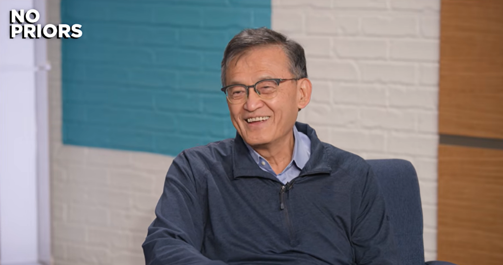
Intel CEO Lip-Bu Tan used his first appearance on the No Priors podcast to describe a wide-ranging plan to reshape Intel’s technology roadmap and business execution. Tan said his goal for Intel is to deliver a “10x” return over five to ten years. In his view, the path is not limited to defending Intel’s traditional PC client base. It also runs through data center CPUs, foundry services, edge computing, physical AI, agentic AI, advanced packaging and new semiconductor materials.
Tan said Intel has already generated roughly a 6x return for shareholders over the past 14 months, but he framed that as only the beginning. He expects the company’s broader potential to become clearer around 2030 to 2032, after Intel has rebuilt core capabilities, improved foundry execution and integrated its XPU, packaging and manufacturing strengths into customized chip solutions for different workloads.
Why Tan Took the Intel Job
Asked why he took on what the host described as one of the hardest jobs in the U.S. semiconductor industry, Tan said he is 66 and that many people thought he should retire rather than accept such a difficult role. He gave two reasons for taking the position: Intel is an iconic company that matters deeply to the semiconductor ecosystem and to the United States, and after Cadence he wanted to do “one more big thing.”
Tan also recounted one of the most surprising episodes of his first year. He said President Donald Trump asked him to resign early one morning, citing a conflict of interest. Tan said he first put his personal emotions aside and reminded himself that he did not need the job and was doing it to save Intel. He then secured a meeting on Thursday morning and another on Monday. During those conversations, he explained that he was born in Malaysia, grew up in Singapore, graduated from MIT and had lived in the United States ever since. Tan said Trump listened and gave him the opportunity to continue.
For Tan, “saving Intel” began with culture. He said he wanted to clarify accountability, speed up decisions and remove layers of bureaucratic meetings. Coming from a startup and venture background, he said he was used to moving at light speed. He also placed all engineering teams under his direct reporting line because he is an engineer and wanted to know personally where problems existed and what needed to be corrected. Listening to customers, simplifying the product line and setting a clear five- to ten-year roadmap became the early operating priorities.
The Crawl-Walk-Run Framework
Tan repeatedly described Intel’s transformation through his “crawl-walk-run” framework. The first step was repairing the balance sheet, which he said had been in poor shape. He welcomed the U.S. government becoming a large shareholder and said he explained to Trump that, as in Japan and Singapore, semiconductor capability should be treated as infrastructure that deserves government support.
He also thanked Nvidia CEO Jensen Huang, whom he called an old friend, for investing $5 billion in Intel. Tan said that investment has now grown to $25 billion or more. SoftBank founder Masayoshi Son, with whom Tan had worked through SoftBank’s board, also stepped in to help. Tan said those moves helped stabilize Intel’s balance sheet and gave the company room to focus on products and execution.
On the product side, Tan said agentic AI and inference workloads are driving strong demand for CPUs. In the past, the ratio between CPUs and GPUs in training-oriented systems was around one to eight. Tan said he now sees that moving toward one to four and even lower. He said AI model developers told him CPUs perform better in reinforcement learning and in coordinating and scheduling many agents quickly. That shift has made Intel’s data center server CPU business an important foundation for the company’s broader plan.
Tan said the company is also moving toward full-stack solutions. Some customers no longer ask only for silicon; one directly asked him to provide “the whole rack.” That means Intel must combine chips, software and system-level capability. Tan said he has been quietly recruiting the best people he can find and added that he personally handles recruiting rather than relying on search firms.
Foundry Execution: Trust, Yield and Cycle Time
Intel’s foundry business has been questioned by outsiders because of its capital intensity and execution difficulty, but Tan said he chose to keep investing in it. His reasoning is that advanced manufacturing in the United States is strategically important for supply-chain security. Large semiconductor companies, he said, cannot rely entirely on one or two geographically concentrated suppliers.
Tan said foundry is both a service business and a business of trust. Before a customer hands over wafers, it must trust the manufacturer. If yield misses the target, customers lose revenue and leave, and winning them back becomes extremely difficult. For that reason, he is focused on yield, defect density and cycle time. He also emphasized the need for the right IP portfolio, such as low-power IP for mobile customers.
Intel has already put 18A into production, and Tan described it as a 1.4-nanometer-class process. He said Intel is also planning for 1 nanometer and 0.7 nanometer. At the same time, he acknowledged that the company remains far behind TSMC in foundry and must stay humble while improving IP, yield, defect density and cycle time. He described TSMC as a partner rather than just a competitor and said the whole industry needs more capacity to serve customers.
Terafab and the Collaboration With Elon Musk
Tan also discussed Intel’s Terafab collaboration with Elon Musk. He said both he and Musk share the view that semiconductor infrastructure has not kept pace with AI growth in capacity, production efficiency or power efficiency. Under the Terafab framework, Musk decided to build his own wafer fab, while Intel provides technology and process support to help accelerate production.
Tan said he meets with Musk’s team every week and described the collaboration as energizing. He praised Musk’s tendency to challenge convention and ask why every step has to be done in a traditional way. Tan mentioned one example: Musk had raised the idea of allowing smoking in certain areas of a cleanroom. Tan said he would not go that far, but added that some areas might be open to discussion and that the key is to keep an open mind while carefully evaluating operational ideas.
On the broader semiconductor supply chain, Tan said AI will have an impact greater than the internet and will reshape many parts of the industry. He listed several bottlenecks: some countries lack enough power, helium has a significant effect on semiconductor manufacturing, memory shortages are the most urgent issue, and new capacity takes years to come online even after expansion begins. CPUs and GPUs are also in short supply, and higher prices eventually flow through to clients.
Advanced Packaging and New Materials
Tan said traditional process-node scaling is getting closer to physical limits. Intel has 18A, is pushing 14A into mass production and can see a path to 10 nanometers and 7 nanometers, but he said that path will become more expensive and more difficult. That is why he is putting more emphasis on materials science, advanced packaging and collaboration with substrate and equipment partners.
In advanced packaging, Tan compared TSMC’s CoWoS with Intel’s next-generation EMIB approach. His priority is ensuring that EMIB can reach customer-required yields at production scale. Intel has also announced advanced packaging manufacturing cooperation projects in India and New Mexico in the United States.
Tan said he has invested in gallium nitride, silicon carbide and indium phosphide. Some of those investments have already been acquired by large semiconductor companies such as ADI. In packaging materials, he has turned to glass because of its heat-dissipation and insulating properties, and he invested in a company called 3DGS. Intel has roughly 1,000 patents in modules, and Tan said integrating substrates and modules is a central engineering problem.
He is also looking at synthetic diamond. Tan said he invested in a diamond wafer company and sees diamond as another strong insulating material for chip packaging. He summarized the mindset with a direct line: “The engineer’s spirit is like this — you keep running into bottlenecks, and then you find a way to cross them or go around them.”
Tan also discussed Moore’s Law in more nuanced terms. The essence is doubling transistor density, but power consumption and cost do not necessarily fall at the same rate. Performance can double, but area and cost do not automatically improve in proportion. Unless new materials and new design methods are found, scaling alone will not deliver the same historical gains. That is why he is hiring more materials science talent and treating the field as a core area of innovation.
Semiconductor Investing, Cadence and AI-Driven Design
Tan brought his venture capital background into the discussion. He said venture and entrepreneurship are in his blood and cited a record of 159 IPOs and 126 M&A exits. He has made more than 200 semiconductor investments, 38% of them in the United States. His investment framework starts with a simple question: where is the bottleneck, and what problem is being solved?
He cited Cradle Semiconductor as an investment tied to interconnect bottlenecks and Celestial AI as an investment focused on optical interconnect inside clusters. Tan said Jensen Huang has invested in almost every photonics-related company, and he did not view that as a coincidence. He also sees major opportunities in EDA, where AI and machine learning can reduce complexity and improve design quality. Power management is another bottleneck he watches closely, especially the large losses involved in converting from 40V to 1V.
Tan said he looks for real customer pain and pays close attention to the first target customer. He prefers hyperscale customers because they have the capacity and willingness to pay millions over several years if they like a product, and landing one large customer can allow a startup to scale. He also highlighted talent in the United States, Silicon Valley, Austin and Israel. He praised Israeli founders for their resilience, including continuing meetings during wartime and moving to audio calls from shelters when alerts sounded.
His experience at Cadence remains central to his thinking. Tan spent nearly 15 years there and said one of his proudest achievements was identifying and training his successor, who is now actively bringing agentic AI into tools to improve efficiency. He said Synopsys’s Sassine is doing similar work, supported by a $2 billion investment from Nvidia, while Synopsys has also acquired Ansys to expand toward full-system design. Tan said large companies are working on AI design tools, but startups still have room to pursue more disruptive paths, either toward IPOs or acquisitions by the two major companies.
Capital, Teams and the Investor Misunderstanding Around Intel
Tan also described how capital formation is changing for infrastructure-heavy businesses. Some venture firms are now willing to put $1 billion into a single company, something he said was previously unimaginable. For AI factories and foundries, he said companies need government funding, sovereign wealth funds or large infrastructure funds. As the CEO of a public company, he is also trying to focus on investors with a long-term growth orientation rather than investors who ask every quarter when the company will buy back stock.
Inside Intel, Tan said he is rethinking teams for the AI era. During the crawl stage, he recruited some of the best semiconductor talent he could find. Now he is thinking about what software talent is needed to build full-stack capabilities. He noted that many team members are in their 40s and 50s, so he wants to bring in younger people who understand workloads and frontier open-source models. He also said his son has become his teacher on AI and machine learning, and that he learns from him while visiting his grandchildren.
Tan described Intel’s past culture as old-fashioned and spreadsheet-driven. He wants to turn it into an AI-enabled enterprise, not only in design but across the organization. The goal is to combine senior technical talent with AI tools and move beyond using AI only in sales and marketing. Design teams are also being pushed to embrace AI more actively.
Asked what investors misunderstand most about Intel, Tan returned to the crawl-walk-run framework. He said the company is still in the crawl stage, even though people are starting to see some of its potential. PC client remains Intel’s base, but the company is moving toward edge, physical AI and agentic AI. In the past, Intel supplied servers and PCs for humans. Now, Tan said, there is another dimension: millions of agents will need access to compute and software stacks.
Tan closed by tying the discussion back to returns. At Cadence, he said the share price rose from $2.40 and delivered around a 76x return for shareholders during his period from acting CEO to retirement. By the time he completed his executive chairman term, the return was around 85x. Intel is much larger and harder to replicate, but Tan said his venture-capital instinct is to look for 10x opportunities. For Intel, that is the explicit goal he has set for himself: a 10x return over five to ten years.
On the question of where compute will live, Tan said large-scale AI infrastructure construction is justified because workloads continue to grow, and any slowdown is coming from supply-side constraints rather than demand. He also stressed that applications will determine where compute belongs. As in the internet era, when Amazon and Netflix emerged as real applications while others disappeared or were acquired, AI will also go through growth and consolidation. Robotics and defense are examples where edge or client-side compute choices matter, because assumptions about connectivity and on-device capability define what can be built.