
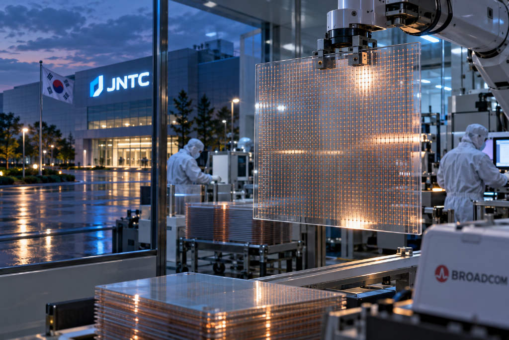
South Korean glass substrate supplier JNTC said it has reduced copper filling time for a 510×515mm, 2mm-thick TGV (through-glass via) substrate from roughly half a day to a full day down to the level of minutes.
Korean media outlet THE ELEC reported on Oct. 6 that JNTC has passed validation by a U.S. semiconductor customer and plans to start mass production of Glass Core substrates in 2027. Industry speculation has pointed to Broadcom as a possible customer.
Why copper filling has been a bottleneck
TGV processing involves drilling fine vias into glass and filling them with copper to connect the top and bottom sides of the substrate. According to the report, even on thinner glass in the 0.8mm to 1.1mm range, defect-free copper filling has typically taken half a day or longer across the industry, making it one of the long-standing barriers to mass production.
JNTC said its approach rests on two main changes. First, it shapes the vias like an hourglass, with a narrower middle section rather than a straight vertical hole, so the copper is mechanically held in place from both ends. Second, it uses an in-house metallization process designed to remove voids and surface sink marks during filling.
The company did not disclose the details of that metallization method, describing it as confidential. The report also did not provide a specific figure behind the “minutes-level” claim, nor did it include yield or cost data.
Why 2mm matters
JNTC said requests for substrates thicker than 2mm are increasing. As more dies are integrated into a single package, substrate area expands as well. Because glass, copper, and insulating materials have different coefficients of thermal expansion, larger formats face a higher risk of warpage or cracking.
In JNTC’s view, increasing glass thickness to 2mm provides the rigidity needed to suppress those defects.
That lines up with earlier industry background cited by ABMedia. Advanced packaging sizes have expanded from 2x reticle to 4x to 5.5x reticle within two years, increasing warpage risk. Glass offers three advantages: adjustable CTE, high rigidity, and a flat surface. At the same time, its hardness also makes it more brittle. Damage to TGV sidewalls, weak copper trace adhesion, and the difficulty of applying conventional optical inspection to transparent materials remain production hurdles.
Validation progress and customer speculation
JNTC reportedly completed development of its 2mm product for a major U.S. semiconductor company in June this year. Product quality was validated by the end customer, while production efficiency was verified by Japanese substrate partner Toppan.
The report said Broadcom is being discussed as a possible end customer because Broadcom and Toppan operate a joint venture in Singapore called AST. It also said another end customer in Taiwan is validating the 2mm product, and a large U.S. technology company recently requested technical cooperation.
Capacity and expansion plans
JNTC currently operates one pilot line at the former Comet site in Hwaseong, Gyeonggi Province, with monthly capacity of about 10,000 to 12,000 units. The company plans to begin mass production of 2mm Glass Core substrates in 2027, and it is also developing a 3mm product.
Separately, JNTC has signed a memorandum of understanding with a local government and plans to invest KRW 347 billion to build a new plant in Gimcheon. Construction is expected to begin in the second half of 2027 to meet customers’ expected initial commercialization demand starting around mid-2028. Once the market moves into large-scale production, the company plans to expand to more than 10 lines.
On the customer side, JNTC said it has signed non-disclosure agreements with 27 companies. Seven of them are end-demand customers, and seven customers have already moved from free samples to paid samples. The company added that no customer has requested exclusive supply and said its long-term goal is to become a customized glass substrate foundry.
Competition across South Korea, China, and Taiwan
JNTC is not alone in pursuing the 2mm segment. THE ELEC said Philoptics recently received orders for 510×515mm, 2mm glass micro-hole laser processing and inspection equipment. LPKF and Taesung also displayed 2mm samples at KPCA 2026, though the industry view cited in the report is that many of these companies are still focused on micro-hole processing and have not solved the time-consuming copper filling step.
Suppliers in Taiwan and China are also active. AUO and Corning previously showed a 510×515mm Glass Core substrate at SEMICON Taiwan 2026, while Innolux is targeting panel-level packaging with a 620×670mm panel format.
In South Korea, Samsung Electro-Mechanics is targeting mass production as early as 2027, while LG Innotek is aiming for 2028. BOE has also shown a TGV Glass Core substrate with an aspect ratio of 15:1.
Commercial adoption remains the next test
On the demand side, the market has circulated claims that Nvidia wants substrate makers to complete glass substrate development within two years and push for adoption before 2028. Whether TSMC introduces glass substrates into its CoWoS lines is seen as a key indicator for broader volume ramp, with estimates cited in the report pointing to late 2028 or early 2029.
If JNTC’s claimed breakthrough holds up, it would give the company an edge in one of the hardest steps in glass substrate manufacturing. Even so, the path from samples to stable shipments still runs through yield improvement and customer qualification.