
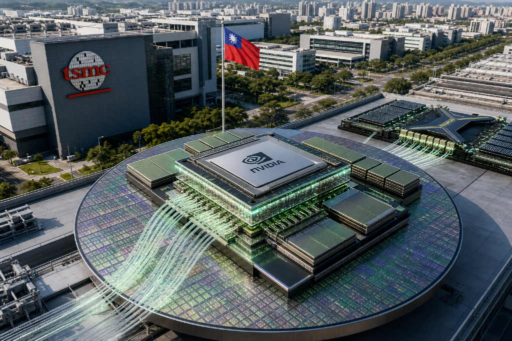
NVIDIA has started development and supply-chain deployment for Feynman, its next-generation AI accelerator platform, even as the Rubin generation has yet to fully ramp, according to a Digitimes report cited by ABMedia. The report says Feynman is expected to use TSMC’s upgraded A16 process, combine it with custom HBM, and bring in co-packaged optics, or CPO, alongside SoIC 3D stacking on a large scale, with mass production targeted for the second half of 2028.
Feynman pushes process, packaging and optical interconnect at the same time
Compared with Rubin, which centered more on multi-chiplet integration and horizontal HBM expansion, Feynman is described as a much harder design problem on both the process and packaging sides. On manufacturing, the platform is said to move directly to TSMC A16. That node builds on N2, or 2 nm, and adds a backside power delivery network, or BSPDN, architecture that the report says can improve power characteristics and signal integrity at the same transistor density.
On packaging, NVIDIA is expected to raise its use of SoIC 3D stacking by a wide margin. Vertical die stacking shortens signal paths, increases bandwidth, and cuts both latency and power use. Feynman is also set to adopt CPO, marking a change in NVIDIA’s interconnect architecture by moving optoelectronic integration from the circuit-board level into the package itself. ABMedia described the jump from Blackwell to Rubin, Rubin Ultra and then Feynman as a steady expansion in technical scope from one generation to the next.
The report’s main point is that Feynman is unusual because it is advancing all three fronts at once: process technology, 3D packaging and optical interconnect. That, in turn, puts far more pressure on TSMC’s ability to integrate multiple advanced technologies into one production path.
NVLink bandwidth is moving past 1 PB/s, making optical links harder to avoid
CPO is being pulled into the Feynman platform because NVLink bandwidth growth is nearing the physical limits of conventional copper interconnect, the report says. Supply-chain figures cited in the story put total bandwidth for a Blackwell NVL72 rack at about 130 TB/s. Rubin rises to 260 TB/s, Rubin Ultra doubles that to 520 TB/s, and Feynman is expected to pass 1,000 TB/s, or more than 1 PB/s.
As AI compute clusters expand from hundreds of GPUs to thousands, the amount of data exchanged between GPUs climbs with them. Copper becomes harder to scale under those conditions because of distance limits, power draw, signal attenuation and heat management. In that setting, optical interconnect starts to look less like an optional upgrade and more like a likely requirement.
To support CPO at production scale, TSMC is advancing its COUPE roadmap. The report says the company plans to use SoIC to stack electronic integrated circuits, or EICs, with photonic integrated circuits, or PICs, in a 3D structure that forms an optical engine. That would shift electro-optical conversion from the board or pluggable-module layer directly into the package.
The report also says the feasibility of mass-producing CPO depends heavily on TSMC’s yield control in SoIC and on its position in the supply chain. In that context, Feynman’s 2028 production target is seen as a key point for the first large-scale commercial deployment of CPO technology.
TSMC is accelerating AP7 and AP8 expansion as SoIC targets move higher
NVIDIA’s shorter product cadence is also creating timing pressure for TSMC’s advanced-node and advanced-packaging expansion. According to the report, TSMC’s packaging build-out is no longer centered only on AP6 in Zhunan and AP5 in Taichung. It has extended to AP7 in Chiayi and AP8 in Southern Taiwan Science Park.
AP8 is currently planned in three phases, P1 through P3, and is mainly focused on CoWoS. AP7 is planned in eight phases. P1 is primarily for Apple WMCM volume production, P2 focuses on SoIC and also includes CPO and CoWoS lines, while P3 and later stages can be configured around customer demand for combinations including SoIC and CoPoS.
ABMedia said TSMC is compressing timelines across the board, from land development and power allocation to cleanroom construction and equipment installation. On SoIC specifically, demand from NVIDIA’s Feynman schedule and from AMD has led TSMC to raise monthly capacity targets several times, from 20,000 wafers by the end of 2026 to 50,000 wafers by the end of 2027.
NVIDIA is pairing technology planning with capital deployment and supplier diversification
The report places Feynman inside a broader NVIDIA strategy tied to AI infrastructure control. Since 2026, NVIDIA has invested more than $40 billion across the AI ecosystem, according to ABMedia. The companies named in the report span AI models, semiconductor manufacturing, cloud data centers and optical communications, including OpenAI, Intel, CoreWeave, Marvell, Lumentum and Coherent.
On the financing side, NVIDIA has also recently formed an AI infrastructure financing platform with Apollo, BlackRock, Blackstone and Goldman Sachs. The target is to mobilize $500 billion in third-party capital to help customers buy GPUs and build data centers.
The supply chain is already feeling the pressure. Even with TSMC expanding aggressively, the report says it still cannot fully absorb market demand. Because of capacity gaps, TSMC yield considerations and customer efforts to spread supplier risk, advanced packaging orders continue to spill over. ASE Technology, listed in the report as 3711, is described as the main recipient of those overflow NVIDIA orders, with a focus on CoWoS and CPO capacity.
Across the wider chain, Feynman’s 2028 production target points to A16, SoIC, CoWoS-L and CPO moving from development validation into production deployment within the same window. For equipment makers and materials suppliers, that would open a new demand cycle spanning process tools, advanced-packaging equipment and optoelectronic materials. The report says stocking and expansion activity across the chain is expected to begin rolling out during 2026 and 2027 and build as Feynman moves closer to production.