
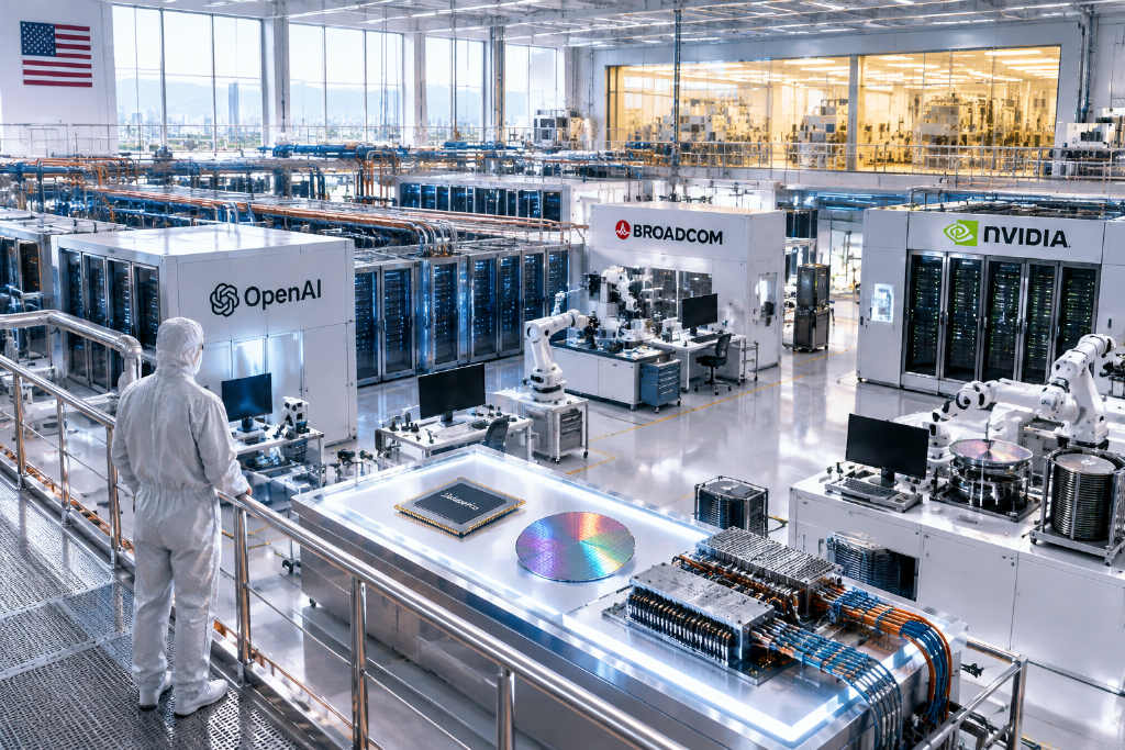
SemiAnalysis said OpenAI’s in-house inference chip Jalapeño beat Nvidia’s current flagship Blackwell on token throughput per megawatt in laboratory testing, and in some comparisons even topped the next-generation Rubin family. The chip went from design to tape-out in about 16 months and was built as OpenAI’s first-generation ASIC in partnership with Broadcom.
A 16-month path from project start to tape-out
The report says OpenAI had been quietly developing Jalapeño over the past two years and formally disclosed it at Hot Chips 2026. SemiAnalysis wrote that development started in mid-2024, and that the period from hiring the team to manufacturing tape-out took roughly 16 months, an unusually short cycle for an ASIC effort.
SemiAnalysis said first-generation chips usually struggle to emerge as serious competitors, but argued that Jalapeño followed a different path. In its account, the chip outperformed every Nvidia, AMD, and Google processor the firm was able to test across several leading open-source models. The report attributes that result to OpenAI’s tight hardware-software co-design and to a strategy centered on building a general-purpose inference chip rather than over-optimizing for one narrow workload.
Token throughput per megawatt came in ahead of Blackwell
SemiAnalysis said it was invited into the lab and verified Jalapeño’s benchmark results using the InferenceX suite. Based on the figures it published, Jalapeño led all rivals on token throughput measured against total power draw per megawatt.
The report adds an important qualification: Jalapeño achieved those numbers without multi-token prediction, or MTP, while the other chips shown in the chart all had MTP enabled.
- On DeepSeek R1, at concurrency 1, the chip delivered more than 700 tokens per second per user
- On Kimi-K2.5 and GPT-OSS, it posted about 1,400 tokens per second per user
- Across all models, GSM8k evaluation results were in line with Nvidia chips
SemiAnalysis said a fairer comparison is single-token prediction. On that basis, it wrote, Jalapeño still stayed ahead of every competing chip. The report also said the chip showed strong interactivity in low-concurrency settings without speculative decoding and without separating prefilling from decoding.
SemiAnalysis says Rubin is the real reference point
SemiAnalysis argued that comparing Jalapeño with Blackwell is incomplete and not entirely fair. In its view, the closer peer group is Rubin and other chips that also use HBM4.
The report says Vera Rubin systems have already started shipping to customers, while Jalapeño remains at the engineering-sample stage and is still some distance from mass production. SemiAnalysis added that it had expected a custom chip like Jalapeño to move past Blackwell. It cited Vera Rubin NVL72 as delivering 5.4x the performance per watt of GB200 NVL72. Even against Rubin, however, SemiAnalysis said Jalapeño still led on STP token throughput per megawatt and exceeded Vera Rubin’s MTP result.
Why tok/s/MW is becoming the key metric
The report says OpenAI designed around performance per watt because its main constraint is data center power, not budget or available building space. In that setup, the number of tokens produced per megawatt becomes critical.
At Computex 2026, Nvidia CEO Jensen Huang said, 「If you have 1 gigawatt of power, then throughput per watt is revenue.」
SemiAnalysis said operators cannot easily secure additional megawatts. The time needed to add more GPUs does not match the time needed to expand grid capacity, and power ceilings at data centers are limited by utility interconnection, infrastructure, cooling capacity, and UPS and backup generation design. The report said this is driving demand for behind-the-meter power capacity, meaning on-site gas turbines and generators, and pointed to xAI’s Colossus 2 as heavily reliant on that setup.
A scale-out network built for up to 2,048 XPUs
OpenAI can connect as many as 2,048 Jalapeño XPUs inside a single scale-out network, according to the report. That network is split into a local domain and a global domain.
- Local domain: 128 chips in a rack connected by backplane, with each XPU offering 4.8Tb/s of one-way bandwidth and all-to-all connections into six 102.4Tb/s Tomahawk 6 ASICs
- Global domain: 16 racks and 2,048 XPUs connected through a mix of copper and optical interconnects, with each XPU carrying 1.6Tb/s of one-way bandwidth on the global link
- The scale-out network accounts for about 10% of total system cost, which the report says preserves optionality for future models in the 10 trillion to 20 trillion parameter range
On the architecture side, OpenAI chose not to split prefilling and decoding across separate chip pools. Draft models and primary models share the same chips and interconnect structure. The report says that choice gives up some theoretical efficiency in exchange for operational flexibility, because workload composition changes over time and fixed allocations for heterogeneous prefilling and decoding silicon can become inefficient later.
Next target: 100MW
The report says Jalapeño is close to producing its first production token, with 100MW set as the next target. It describes the remaining bottlenecks as mostly hardware-related: how many chips can be produced, how well data centers can be deployed and operated, and how monitoring and resilience are handled. On the software side, the report says the stack has already been validated.