


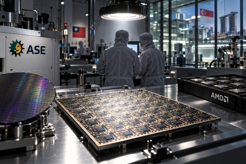
Panel-level packaging (PLP) is moving from technical validation into actual investment, according to ABMedia. Research firm SemiAnalysis said ASE Technology has presented a PLP solution for AMD’s next-generation Venice CPU, with initial mass production targeted for the first quarter of 2027. Separately, Taiwan’s Ministry of Economic Affairs Investment Commission approved Powertech Technology’s plan on the 28th to build operations in Singapore, committing $400 million to panel-level advanced packaging, assembly, and final test foundry services.

Why PLP is drawing attention
Traditional advanced packaging typically uses round wafers, such as 300 mm wafers, as the carrier. But placing square chips or interposers on a circular surface leaves unused corners and creates material loss. PLP uses large square panels instead, allowing more packages to be processed in each batch, improving material utilization, and lowering unit packaging costs through scale.
As AI accelerators and high-speed networking chips demand larger package sizes, stronger signal transmission, and better thermal performance, PLP is being treated as a key direction for advanced packaging. TSMC has also said the next stage of packaging competition will gradually shift from CoWoS to panel-level CoPoS, and it has already started building out the supply chain ecosystem.
That said, several manufacturing hurdles remain before PLP can move into volume production. The article pointed to large-area warpage control, process uniformity, precise alignment, and yield improvement as the main challenges.
ASE and SPIL work with AMD on Venice
SemiAnalysis said ASE and its subsidiary Siliconware Precision Industries (SPIL) have been working with AMD to introduce second-generation Fan-Out Embedded Bridge (FOEB) technology for Venice. Initial mass production is targeted for the first quarter of 2027. Early output may be limited, and the production site is speculated to be in Kaohsiung.
On the numbers, a 310 × 310 mm panel can fit 25 Venice interposers after edge loss is taken into account, compared with 22 on a traditional 300 mm round carrier. That lifts the total package count by about 14%. Venice uses a 2.7-reticle-size interposer, which SemiAnalysis described as the technical starting point for panel-level interposers.
The report said the larger cost advantage appears with bigger interposers. Using a 9.5-reticle-size example, one panel could produce 9 units, while a wafer would produce only 4, widening the gap to about 2.25x. Reaching that stage, however, still depends on more mature equipment for larger reticle sizes and larger panels.
PTI gets approval for a $400 million Singapore project
On another front, the Investment Commission approved Powertech Technology and Broadcom to establish XCIP TECHNOLOGIES. The business scope covers panel-level advanced packaging, assembly, and final test foundry services. Powertech has historically focused on memory packaging and testing for products such as DRAM and NAND Flash, but in recent years it has been expanding into advanced packaging, FOPLP, and heterogeneous integration to reduce its dependence on memory cycles. In this project, PLP is listed as a strategic priority.
Broadcom has continued to expand its custom AI accelerator and high-speed switch chip business. Increased ASIC spending by cloud companies has also driven demand for advanced packaging capacity and a more diversified supply chain. If Powertech can establish PLP mass-production capability, the company could extend from memory packaging and testing into the supply chain for AI ASICs and high-end logic chips.
TSMC pushes CoPoS as the PLP supply chain takes shape
PLP is not only a battleground for outsourced semiconductor assembly and test companies. TSMC is advancing CoPoS and has also started three-way glass substrate validation with Japanese substrate maker Ibiden and Innolux. According to the article, earlier reporting said test samples showed a 16% improvement in package warpage and a 19% reduction in the coefficient of thermal expansion compared with traditional organic substrates.
TSMC has also said panel-level packaging could complete R&D as early as 2027 and reach the market in 2028, with OSAT partners taking the lead. In other words, foundries, substrate and panel makers, and packaging and testing companies are all moving to secure positions at the same time, with commercialization timelines largely concentrated in 2027 and 2028.