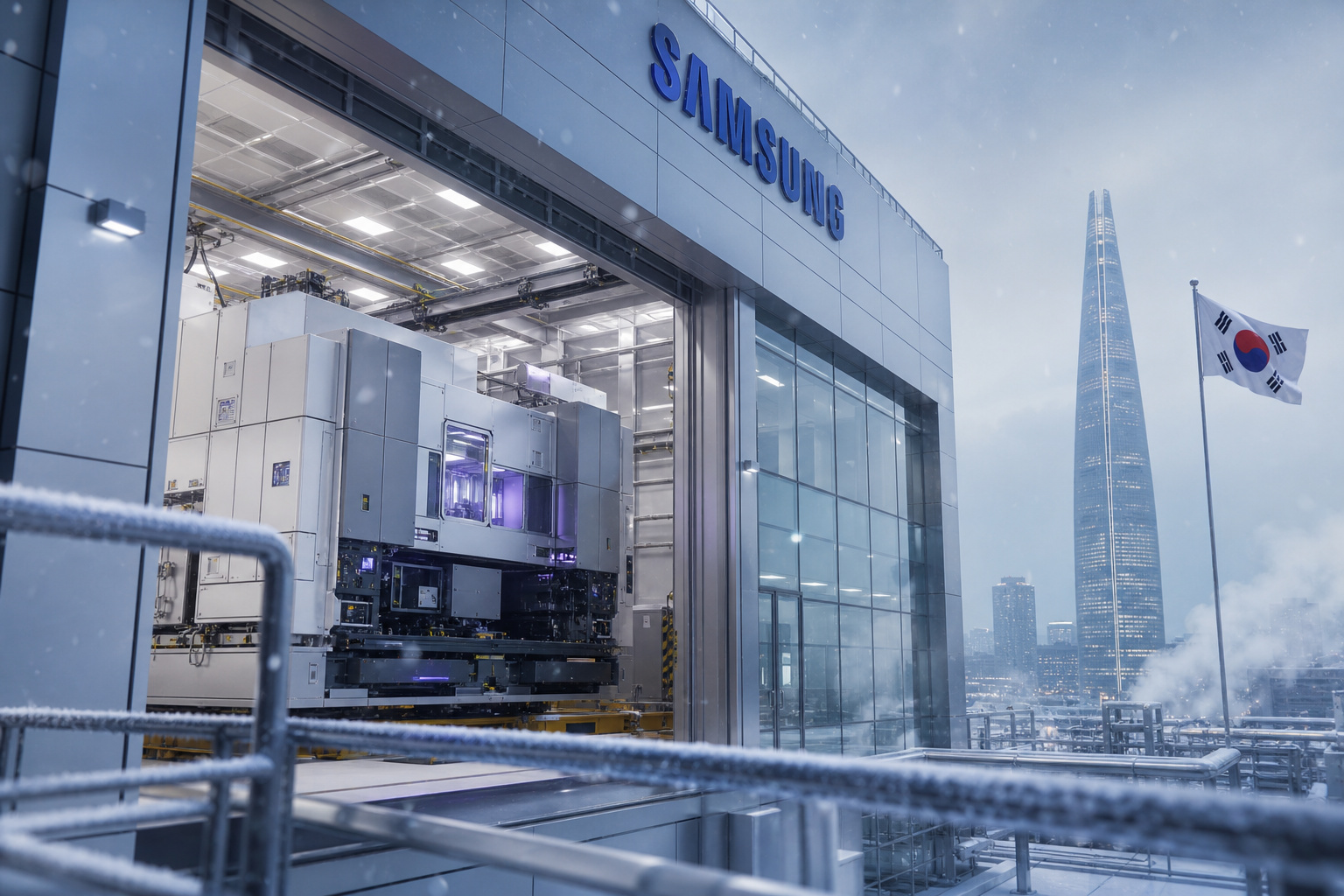
Samsung Electronics plans to adopt High-NA EUV lithography starting with its 1nm (A10) process node, targeting mass production around 2030, according to a ChainCatcher report. The roadmap was outlined by a member of the Foundry process development team at Samsung's Semiconductor Research Institute during the '2026 Next-Generation Lithography + Patterning Academic Conference.' Samsung currently relies on 0.33 NA EUV multipatterning for 2nm and below, and plans to mass-produce 1.4nm in 2029 before moving on to 1nm. High-NA EUV raises the lens numerical aperture from 0.33 to 0.55, delivering higher resolution that could turn multipatterning into a single patterning step. That would help cut manufacturing costs, raise productivity and add design flexibility. The same researcher expects 1.4nm and 1nm to remain on 0.33 NA EUV multipatterning, with High-NA patterning becoming the core technology for the generation that follows. The catch: the technology is hard to master, equipment is expensive, and material technology needs to be upgraded in step.
Samsung Electronics plans to apply High-NA EUV lithography starting with its 1nm (A10) process node, targeting mass production around 2030, according to ChainCatcher.
Piao Changmin, from the Foundry process development team at the Samsung Semiconductor Research Institute, disclosed the plan at the '2026 Next-Generation Lithography + Patterning Academic Conference.' Samsung currently uses 0.33 NA EUV multipatterning for 2nm and below.
Under the company's current roadmap, 1.4nm production is scheduled for 2029, with 1nm to follow. Piao expects 1.4nm and 1nm to remain on 0.33 NA EUV multipatterning, then High-NA patterning will take over as the core technique for the next generation of process technology.
High-NA EUV lifts the lens numerical aperture from 0.33 to 0.55, delivering higher resolution. Ultra-fine processes that previously required multipatterning can be done in a single patterning step, which helps lower manufacturing costs, raise production efficiency and add design flexibility.
The technology still comes with serious hurdles. Equipment is expensive, the process is technically demanding, and material technology needs to be upgraded in step.
This article was originally published by Bit.Fan. For more cryptocurrency news and market insights, visit www.bit.fan. Disclaimer:
The market information, project data, and third-party content displayed on this platform are for industry information sharing only and do not constitute any form of investment advice or return commitment.
Cryptocurrency trading carries high risks. Users should fully assess their risk tolerance and make independent decisions. All profits, losses, and legal responsibilities are borne by the users themselves.