
Intel and Samsung publish separate High-NA EUV updates
ASML issued separate updates with Intel and Samsung Electronics in the same week on progress in High-NA EUV lithography. According to a joint statement from Intel Foundry and ASML, the companies said at the SPIE Mask Technology and Extreme Ultraviolet Lithography conference that High-NA EUV has processed more than 1 million wafers cumulatively.
That total covers tool verification and testing, research and development, and volume manufacturing for selected layers of Intel Core Ultra Series 3 processors, codenamed Panther Lake. Intel and ASML said clearly that the number does not represent 1 million commercial Panther Lake wafers, and they did not disclose how testing, R&D, and production were split within the total.
The product uses Intel 18A. Intel said High-NA met Intel Foundry expectations for overlay accuracy, throughput, and availability, and that some Intel 18A layers performed on par with or better than comparable conventional EUV layers. The company did not publish quantified data on yield, overlay accuracy, defect density, or throughput.
ASML President and Chief Executive Officer Christophe Fouquet said Intel Foundry is one of the key leaders in introducing High-NA, from installing the first commercial EXE system in 2024 and completing validation of the latest-generation tool to shipping the first volume logic product manufactured with High-NA. Intel Executive Vice President Naga Chandrasekaran said companies building increasingly complex AI products need manufacturing innovation that can go straight into production and be practical to use.
Samsung sets a 2028 timetable for DRAM
Samsung Electronics and ASML said in an announcement released the same day that they are expanding their strategic collaboration. Under that plan, Samsung aims to introduce High-NA EUV into future DRAM mass production in 2028. According to the companies, this is the first time a memory maker has committed to a timetable for using High-NA in production.
The companies said the higher resolution of High-NA could simplify process steps and extend the DRAM scaling roadmap.
ABMedia added that Chain News had previously reported that SK hynix was said to be considering Intel foundry services for HBM4E base dies, a sign that foundry and equipment choices in advanced process technology are becoming less fixed among memory makers.
Masks move from 6 inches toward 12 inches
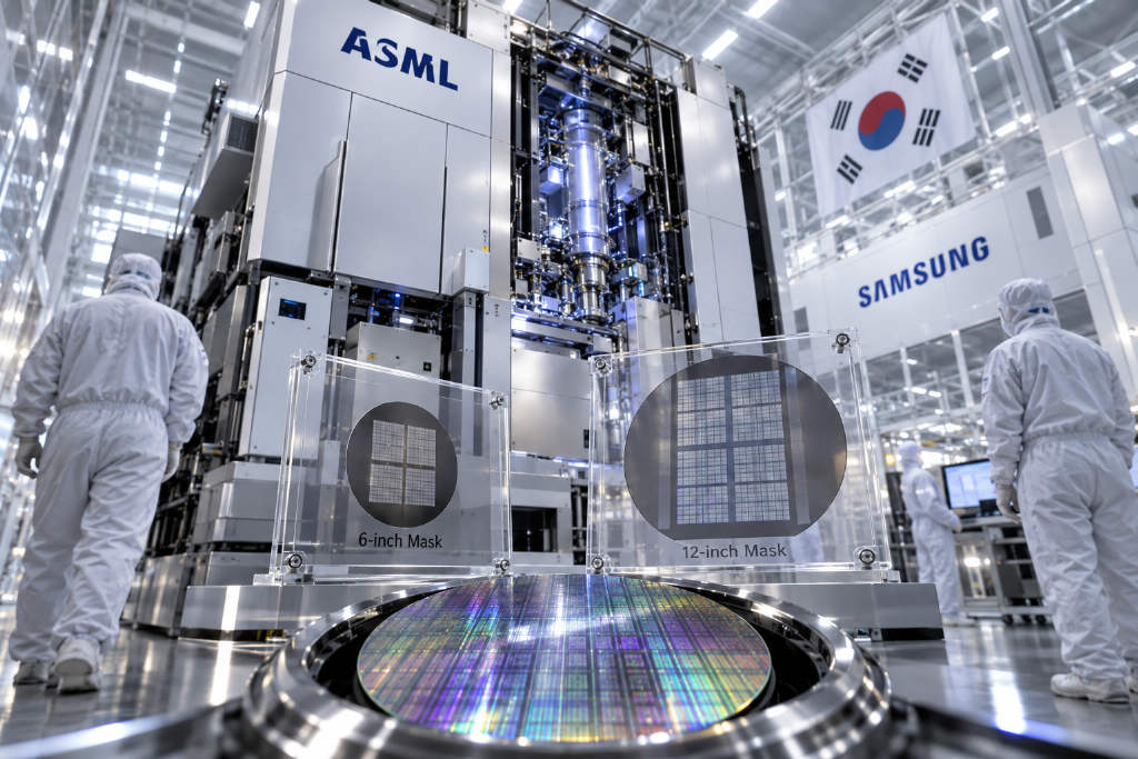
The two announcements also point to the same infrastructure change. Intel said it has spent three years advancing a large-mask initiative and has worked with ASML and industry partners on standards that support a transition to 6x12-inch masks while keeping existing 6-inch masks usable. Samsung said it is joining the industry initiative to advance next-generation 12-inch mask technology.
Moving from the long-used 6-inch mask standard toward 12 inches is expected to improve fab productivity, lower manufacturing costs, and remove stitching limits. Intel Foundry and ASML also scheduled two presentations at the conference covering mask stitching technology.
High-NA specifications
On the technical side, High-NA raises the numerical aperture from 0.33 to 0.55, reaches 8 nm resolution, and delivers 40% higher image contrast than current NXE systems. The system referenced in the report is the TWINSCAN EXE:5200B.